
Method for growing rhenium disulfide nanometer sheets on silicon substrate of non-oxidation layer

A rhenium disulfide and silicon substrate technology, applied in chemical instruments and methods, inorganic chemistry, rhenium compounds, etc., can solve problems such as morphology, structural damage, troubles, etc., and achieve the effect of overcoming direct growth

Active Publication Date: 2018-10-23
INT ACAD OF OPTOELECTRONICS AT ZHAOQING SOUTH CHINA NORMAL UNIV
View PDF6 Cites 9 Cited by
  • Summary
  • Abstract
  • Description
  • Claims
  • Application Information

AI Technical Summary

Problems solved by technology

And currently, ReS 2 Nanosheets can only be synthesized on materials such as silica, mica, gold foil, graphene, etc. If the ReS synthesized on these substrates 2 Applications to silicon-based optoelectronic devices or catalytic hydrogen production need to be transferred to the target substrate by various means. There is no doubt that this process will cause damage to its morphology, structure, etc., and at the same time bring some unpleasant effects. necessary trouble
Therefore, ReS 2 Applications in these areas have been limited to a certain extent

Method used


Image

  • Method for growing rhenium disulfide nanometer sheets on silicon substrate of non-oxidation layer
  • Method for growing rhenium disulfide nanometer sheets on silicon substrate of non-oxidation layer
  • Method for growing rhenium disulfide nanometer sheets on silicon substrate of non-oxidation layer

Examples


Embodiment 1

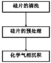
[0036] 1. A method for growing rhenium disulfide nanosheets on a silicon substrate without an oxide layer, which is prepared by chemical vapor deposition, and the preparation process is as follows figure 1 shown.

[0037] Materials used are: 500 mg sublimated sulfur (aladin, 99.99%), 1.5 mg ReO 3(aladin, 99.9%); hydrofluoric acid (Tianjin Damao Chemical Reagent Factory), three-temperature zone tube furnace (Hefei Kejing Material Technology Co., Ltd., OTF-1200X-Ⅲ), argon (purity 99.999%) .

[0038] Concrete preparation process is as follows:

[0039] (1) Cleaning the silicon substrate: Cut a commercially available circular silicon wafer without an oxide layer into small pieces of 2.5 cm*2.5 cm, and then ultrasonically clean them in the order of acetone, ethanol, and deionized water for 10 min each, with an ultrasonic power of 180 W. Frequency 40KHz.

[0040] (2) Pretreatment of silicon substrate: soak the cleaned silicon wafer in a certain concentration of hydrofluoric acid...


PUM


Abstract

The invention discloses a method for growing rhenium disulfide nanometer sheets on a silicon substrate of a non-oxidation layer. The method comprises the following steps that S1, the silicon substrateis cleaned and is subjected to pretreatment; S2, in a multi-temperature-zone tubular furnace, one aluminum oxide boat is arranged in each of two adjacent temperature regions, wherein the distance between the two aluminum oxide boats is 20 to 30cm; a sulfur source is arranged in the center position of the aluminum oxide boat in the upper stream temperature region; a rhenium source is arranged in the lower stream edge of the aluminum oxide boat of the lower stream temperature region; a growth surface of the silicon substrate faces the downward position; the distance from the silicon substrate to the lower stream edge of the aluminum oxide boat of the lower stream temperature region is 0 to 1cm; S3, then, inert gas is introduced into a dual-temperature-region tubular furnace, heating is performed for reaction; the rhenium disulfide nanometer sheets can grow on the silicon substrate of the non-oxidation layer. The sublimed sulfur is used as a sulfur source; rhenium trioxide is used as a rhenium source; a chemical gas phase precipitation method is used; by regulating the distance between the sulfur source and the rhenium source and the position of the rhenium source in the lower streamtemperature region and the position of the silicon substrate, the rhenium disulfide nanometer sheets on the silicon substrate can directly grow on the silicon substrate of the non-oxidation layer.

Description

technical field [0001] The invention relates to the technical field of nanomaterial preparation, in particular to a method for growing rhenium disulfide nanosheets on a silicon substrate without an oxide layer. Background technique [0002] Two-dimensional transition metal chalcogenides (TMDs) have a graphene-like structure and have excellent electrical, optical, magnetic, and mechanical properties, and have become one of the hotspots in material science research today. Rhenium disulfide (ReS 2 ) is a "new star" in this family of materials in recent years, and most of the studied similar materials with high lattice symmetry (such as MoS 2 、WS 2 etc.) show isotropic difference, due to the presence of Paiworth distortion, ReS 2 The degree of asymmetry is higher in the structure, and it has a unique twisted 1T phase, so that it has anisotropy in electrical and optical properties. and ReS 2 Has a very weak interlayer coupling effect, so that no matter single-layer or multi-...

Claims


Application Information

Patent Timeline
Patent Type & Authority Applications(China)
IPC IPC(8): C01G47/00
CPCC01G47/00C01P2002/82C01P2002/85C01P2004/03
Inventor 张璋黄文添李婧
Owner INT ACAD OF OPTOELECTRONICS AT ZHAOQING SOUTH CHINA NORMAL UNIV
Learn More