
Manufacturing method and application of oxide semiconductor thin film

A technology of oxide semiconductors and production methods, which is applied in semiconductor/solid-state device manufacturing, semiconductor devices, transistors, etc., can solve the problems of unfavorable preparation of high-performance thin-film transistors and poor performance of thin-film transistors, and avoid vacuum equipment and photolithography. process, meeting high pixel requirements, and reducing production costs

Inactive Publication Date: 2018-10-23
SUZHOU INST OF NANO TECH & NANO BIONICS CHINESE ACEDEMY OF SCI
View PDF7 Cites 0 Cited by
  • Summary
  • Abstract
  • Description
  • Claims
  • Application Information

AI Technical Summary

Problems solved by technology

Experiments have shown that when the contact angle of the substrate surface is greater than 30°, the size of the oxide semiconductor film can be reduced to less than 30 μm, but at this time its thickness will be greater than 100 nm, and the performance of the prepared thin film transistor is very poor, indicating that thicker oxide semiconductor films Thin films are not conducive to the preparation of high-performance thin-film transistors

Method used


Image

  • Manufacturing method and application of oxide semiconductor thin film
  • Manufacturing method and application of oxide semiconductor thin film
  • Manufacturing method and application of oxide semiconductor thin film

Examples


Embodiment 1

[0045]This embodiment provides a method for fabricating an oxide semiconductor thin film, which includes the following steps:

[0046] S1. Perform hydrophobic treatment on the substrate to obtain a modified substrate.

[0047] Generally speaking, after the substrate is cleaned, it can be modified by hexamethyldisilazine (HMDS for short), that is, hydrophobized, and a modified substrate with a contact angle of 52°±4° can be obtained.

[0048] In this embodiment, a silicon wafer containing thermally oxidized silicon dioxide with a thickness of 300 nm is specifically selected as the substrate; other optional materials for the substrate will not be described in detail here, and those skilled in the art can refer to the prior art to select according to specific requirements. Can.

[0049] S2. Prepare electronic ink.

[0050] Specifically, functional reagents are added to the precursor solution of the oxide semiconductor to obtain electronic ink. Among them, the functional reagen...

Embodiment 2

[0074] In the description of Embodiment 2, the similarities with Embodiment 1 will not be repeated here, and only the differences with Embodiment 1 will be described. The difference between Example 2 and Example 1 is that in step S2, the concentration of PVP 1300000 in the electronic ink is 0.05mg / mL, and the precursor solution of the oxide semiconductor is 0.02mol / L In(NO 3 ) 3 aqueous solution.

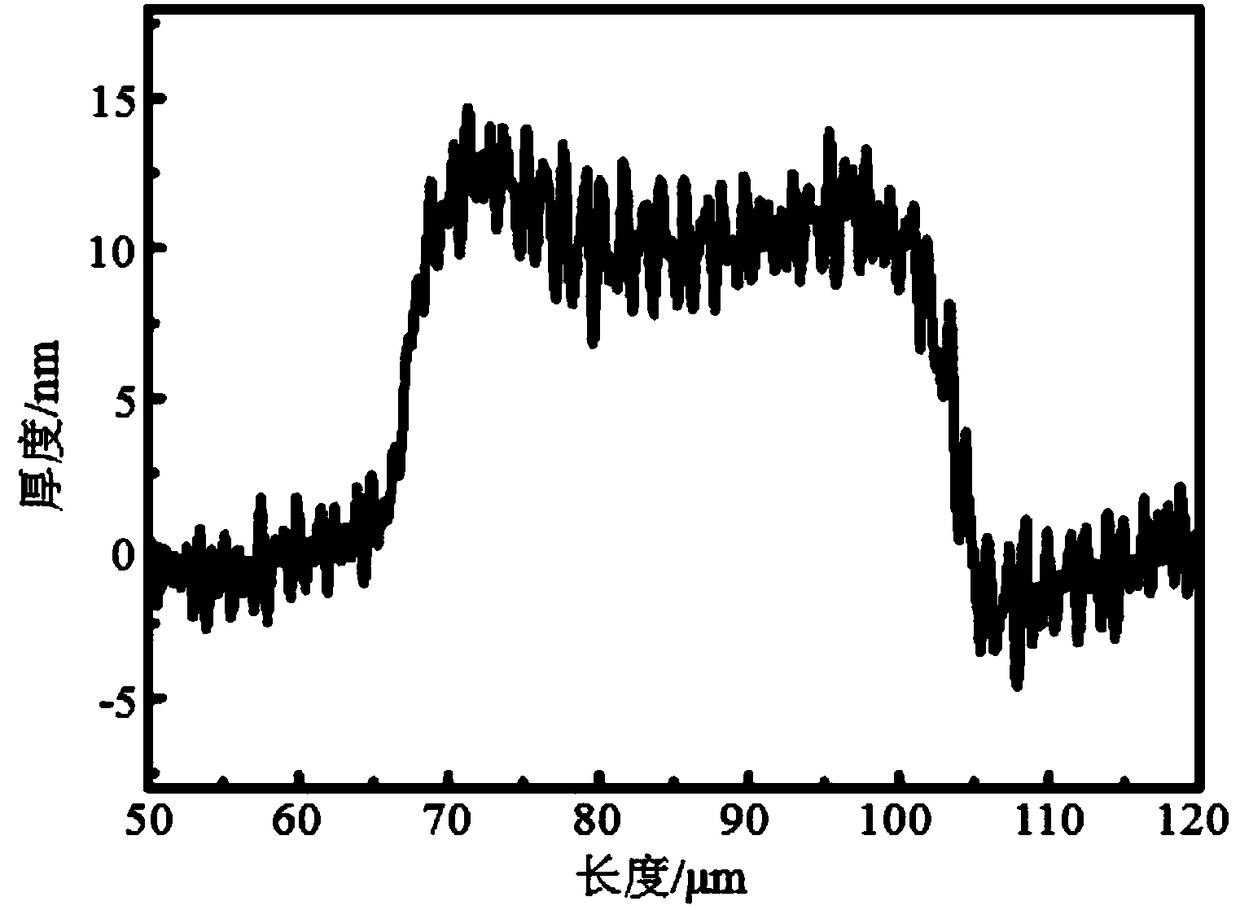
[0075] The oxide semiconductor thin film array obtained in this example has an optical physical map and a film topography map equivalent to those of the oxide semiconductor thin film array in Example 1.

Embodiment 3

[0077] Based on the fabrication method of the oxide semiconductor thin film provided in the above-mentioned embodiment 1 and embodiment 2, a small-sized and thin oxide semiconductor thin film can be fabricated, which can be applied in the field of oxide thin film transistors as active transistors therein. layer to obtain high-performance oxide thin film transistors.

[0078] Specific reference Figure 9 , the oxide thin film transistor provided in this embodiment is a bottom-gate type; the oxide thin film transistor includes a gate 11, a dielectric layer 12, an active layer 13 that are sequentially stacked, and an A source 14 and a drain 15 at both ends, both of which are in contact with the dielectric layer 12 .

[0079] Specifically, the active layer 13 is formed of a small-sized, thin-thick oxide semiconductor film.

[0080] Hereinafter, the method for fabricating the bottom-gate oxide thin film transistor of this embodiment will be described in detail; the method for fab...


PUM


Abstract

The invention discloses a manufacturing method of an oxide semiconductor thin film, which comprises the steps of performing hydrophobic treatment on a substrate to obtain a modified substrate; preparing electronic ink, that is, adding a functional reagent to a precursor solution of an oxide semiconductor to obtain the electronic ink, wherein the functional reagent has hydrophilicity and viscosityenhancement; printing the electronic ink on the surface of the modified substrate to form ink droplets; performing annealing treatment on the ink droplets so as to obtain an oxide semiconductor thin film on the modified substrate. The manufacturing method can form a small and thin oxide semiconductor thin film. Meanwhile, the application of vacuum equipment and a photoetching technology is avoided, and thus the manufacturing cost is effectively reduced. The invention further provides an oxide thin film transistor and a manufacturing method thereof based on the manufacturing method of the oxidesemiconductor thin film. The oxide semiconductor thin film is used as an active layer, and more oxide thin film transistors can be integrated to be maximum extent in a unit area, thereby meeting high-pixel requirements of a display backplane.

Description

technical field [0001] The invention belongs to the technical field of electronic materials and devices, and in particular relates to a method for manufacturing an oxide semiconductor thin film and the application of the oxide semiconductor thin film in an oxide thin film transistor. Background technique [0002] Oxide thin film transistors have become a new generation of display backplane driving technology due to their advantages of good stability and low fabrication temperature. In an oxide thin film transistor, the key structure is an oxide semiconductor thin film. High-performance oxide semiconductor thin films can be prepared not only by vacuum deposition, but also by inkjet printing; among them, the oxide semiconductor thin film is prepared by printing technology, which avoids the use of vacuum equipment and photolithography technology, and has the advantages of simple process and low cost. Etc. [0003] In order to realize a display panel that can drive LCD and OLE...

Claims


Application Information

Patent Timeline
Patent Type & Authority Applications(China)
IPC IPC(8): H01L21/02H01L29/786
CPCH01L21/02554H01L21/02565H01L21/02628H01L29/7869
Inventor 吴绍静张青邵霜霜陈征崔铮
Owner SUZHOU INST OF NANO TECH & NANO BIONICS CHINESE ACEDEMY OF SCI
Learn More