
Eureka
For R&D, Eureka makes reading and utilizing patents & technical documents easy.
Eureka AIR
Designed for self-driven R&D workflows. Generate viable solutions, solve complex R&D challenges, empower your innovation with AI.

Eureka Materials
Designed for material experts only. Revolutionize your material R&D, from search, analyze, to developing new materials.

TechResearch
Generate reliable direction feasibility study reports for your R&D in just a few steps.

TechSeek
Discover and master advanced knowledge NOW. Basics, ideas, possibilities, all at once.

TechMind
As an expert in R&D Theories, TechMind can generates customized viable solutions instantly.

TechRisk
Analyze your overall solution with one click, know your potential R&D risks in advance.

TechMonitor
Get weekly tech updates, stay abreast of the latest tech innovations and key insights.
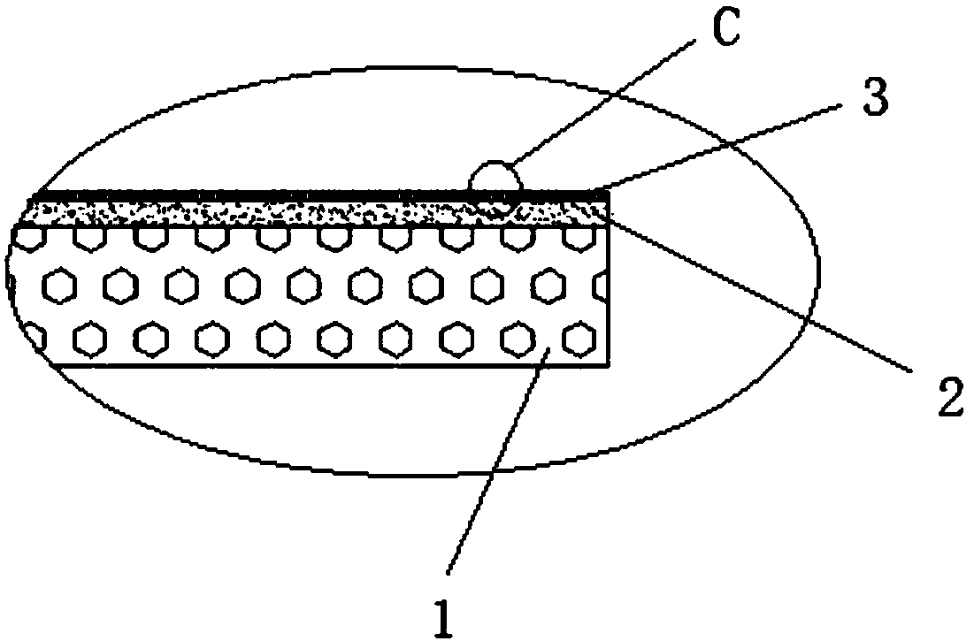
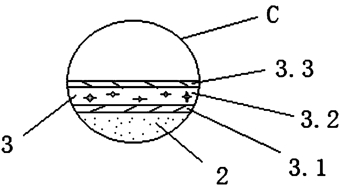
Conductive composite film, ceramic coating method by using conductive composite film and device adopted by ceramic coating method
A composite film and ceramic technology, applied in the field of electronics, can solve the problems of large space occupation, easy detachment of film layer, thick film layer, etc., to achieve the effects of good product performance, improved coating efficiency, and simplified process steps
- Summary
- Abstract
- Description
- Claims
- Application Information
AI Technical Summary
Problems solved by technology
Method used
Image

Examples
Embodiment 1
[0040] A ceramic coating method, the details are as follows:
[0041] The coating device used in this coating method includes: a coating machine, a vacuum device, a fixture, a sandblasting machine and a cleaning machine. The coating machine, the fixture, the sandblasting machine and the cleaning machine are set independently of each other. It includes an A cavity and a B cavity, both of which are connected to the vacuuming device, and the B cavity is provided with a fixed part that drives the clamp to rotate. Here, the coating machine is a magnetron sputtering coating machine; the sandblasting machine is an automatic sandblasting machine; and the cleaning machine is an ultrasonic cleaning machine.
[0042] Above-mentioned ceramic coating method specifically comprises the following steps:
[0043] The pretreatment step is specifically: including sandblasting and cleaning. The sandblasting is specifically: using a sandblasting machine to spray alumina powder on the surface of t...
Embodiment 2
[0059] The difference between this embodiment and embodiment 1 lies in that: the first inactive metal layer and the second inactive metal layer are titanium layers, and the active metal layer is an aluminum layer. The thickness of each layer and the actual process of coating are the same as in Example 1.
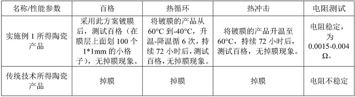
[0060] The product performance that present embodiment obtains is the same as embodiment 1.
[0061] In addition, other inactive metals (copper, silver, etc.) can also be used in the first inactive metal layer and the second inactive metal layer, and other active metals (such as magnesium, potassium, etc.) can also be used in the active metal layer. etc.), and then slightly modify the coating parameters according to the actual situation to meet different needs.
PUM
| Property | Measurement | Unit |
|---|---|---|
| thickness | aaaaa | aaaaa |
| thickness | aaaaa | aaaaa |
| thickness | aaaaa | aaaaa |
Abstract
Description
Claims
Application Information
 - R&D Engineer
- R&D Manager
- IP Professional
- Industry Leading Data Capabilities
- Powerful AI technology
- Patent DNA Extraction
Browse by: Latest US Patents, China's latest patents, Technical Efficacy Thesaurus, Application Domain, Technology Topic, Popular Technical Reports.
© 2024 PatSnap. All rights reserved.Legal|Privacy policy|Modern Slavery Act Transparency Statement|Sitemap|About US| Contact US: help@patsnap.com