

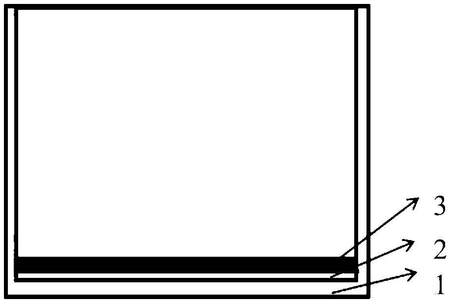
Crucible using silicon nitride film as resisting layer and used for pseudo-single crystal silicon cast ingot
A technology of silicon nitride film and quasi-single crystal silicon, which is applied in the field of crucibles for quasi-single crystal silicon ingot casting, can solve the problems of increasing the cost of ingot casting and the limited effect of the width of the red zone at the bottom of the silicon ingot, and achieves improved utilization rate, The red zone width is low and the effect of increasing the minority carrier lifetime
- Summary
- Abstract
- Description
- Claims
- Application Information
AI Technical Summary
Problems solved by technology
Method used
Image

Examples
Embodiment 1
[0026] (1) Provide a crucible with an inner diameter of 175*175mm and a height of 190mm, and coat the inner bottom of the crucible with a silicon nitride coating;
[0027] (2) On a solar-grade monocrystalline silicon wafer with a thickness of 0.2mm and a specification of 170*170mm;
[0028] (3) Deposit a silicon nitride film with a thickness of 100nm on the above-mentioned solar-grade monocrystalline silicon wafer by PECVD method, and paste it on the inner bottom of the crucible through high-purity silica sol,
[0029] Among them, the process parameters of PECVD method are: deposition temperature is 350°C, deposition time is 10min, deposition pressure is 120Pa, radio frequency power is 20W, total gas flow rate is 3400sccm;
[0030] Wherein, the volume ratio of ammonia and silane is 10:1;
[0031] (4) Then set the seed crystal on the bottom barrier layer of the quasi-single crystal silicon ingot crucible using the silicon nitride film as the barrier layer, and then set the sil...
Embodiment 2
[0035] (1) Provide a crucible with an inner diameter of 175*175mm and a height of 190mm, and coat the inner bottom of the crucible with a silicon nitride coating;
[0036] (2) On a solar-grade monocrystalline silicon wafer with a thickness of 0.2mm and a specification of 170*170mm;
[0037] (3) Deposit a 100nm silicon nitride film with a thickness of 100nm by PECVD on the above-mentioned solar-grade monocrystalline silicon wafer, and paste it on the inner bottom of the crucible through high-purity silica sol;
[0038] Among them, the process parameters of PECVD method are: deposition temperature is 400°C, deposition time is 6min, deposition pressure is 180Pa, radio frequency power is 40W, total gas flow rate is 4500sccm;
[0039] Wherein, the volume ratio of ammonia and silane is 6:1;
[0040] (4) Then set the seed crystal on the bottom barrier layer of the quasi-single crystal silicon ingot crucible using the silicon nitride film as the barrier layer, and then set the silico...
Embodiment 3
[0044] (1) Provide a crucible with an inner diameter of 175*175mm and a height of 190mm, and coat the inner bottom of the crucible with a silicon nitride coating;
[0045] (2) On a solar-grade monocrystalline silicon wafer with a thickness of 0.2mm and a specification of 170*170mm;
[0046] (3) Deposit a silicon nitride film with a thickness of 200nm on the above-mentioned solar-grade monocrystalline silicon wafer by PECVD method, and paste it on the inner bottom of the crucible through high-purity silica sol;
[0047] Among them, the process parameters of PECVD method are: deposition temperature is 450°C, deposition time is 12min, deposition pressure is 160Pa, radio frequency power is 30W, total gas flow rate is 4000sccm;
[0048] Wherein, the volume ratio of ammonia and silane is 8:1;
[0049] (4) Then set the seed crystal on the bottom barrier layer of the quasi-single crystal silicon ingot crucible using the silicon nitride film as the barrier layer, and then set the sili...
PUM
| Property | Measurement | Unit |
|---|---|---|
| thickness | aaaaa | aaaaa |
| height | aaaaa | aaaaa |
| width | aaaaa | aaaaa |
Abstract
Description
Claims
Application Information