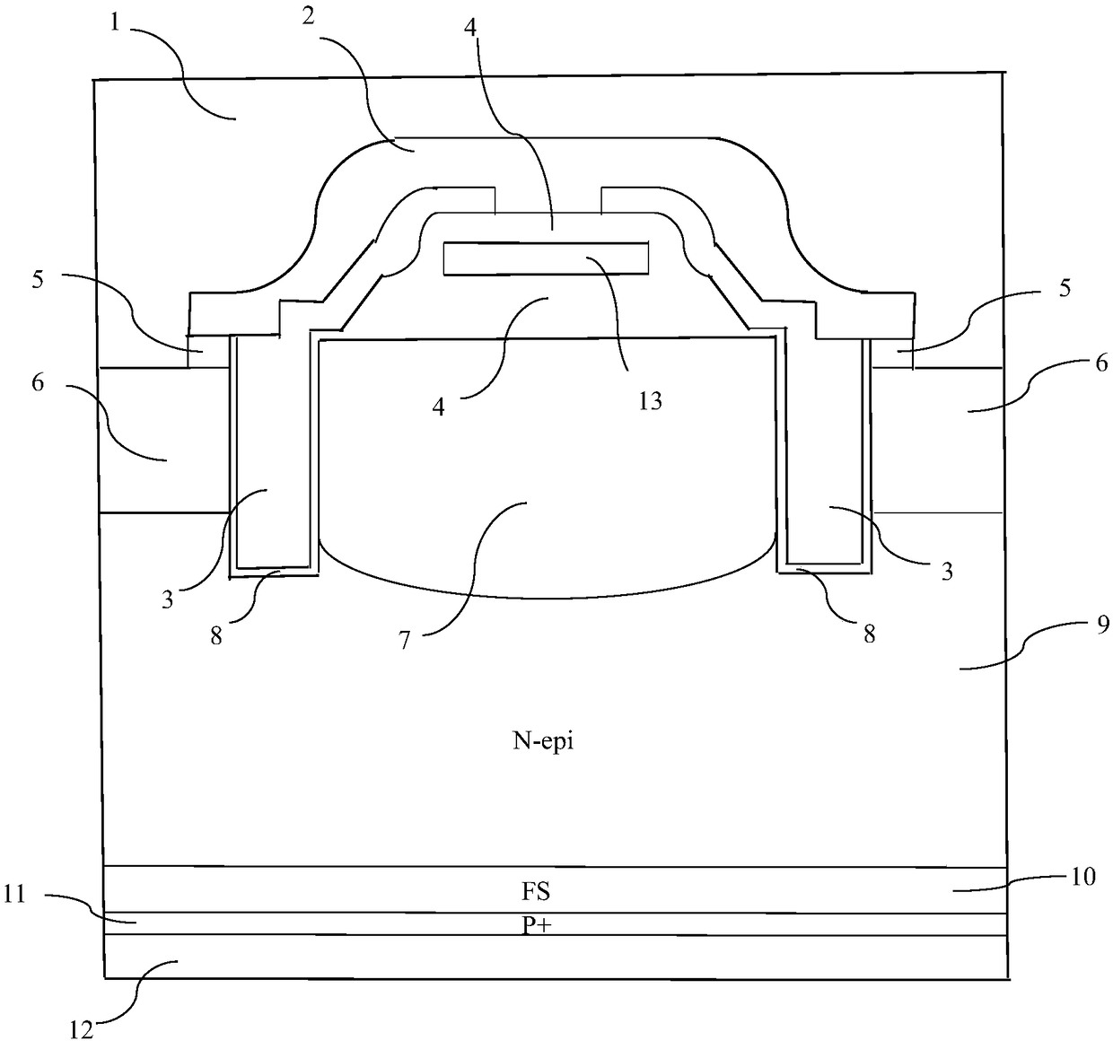
Groove-type IGBT device with shield grid
A shielded gate, trench technology, applied in semiconductor devices, electrical components, circuits, etc., can solve problems such as irreversible damage, and achieve the effect of reducing switching loss, reducing capacitance, device input capacitance and feedback capacitance.
- Summary
- Abstract
- Description
- Claims
- Application Information
AI Technical Summary
Problems solved by technology
Method used
Image
Examples
Embodiment Construction
[0024] The present invention will be further described below in conjunction with specific drawings and embodiments.
[0025] Such as figure 1 Shown: in order to improve the withstand voltage of the device, reduce the parasitic capacitance of the device, and reduce the switching loss, taking the N-type IGBT device as an example, the present invention includes a semiconductor substrate and a cell region located at the center of the semiconductor substrate, and the semiconductor substrate includes N -type epitaxial layer 9 and the P-type base region 6 located in the upper part of the N-type epitaxial layer 9;
[0026] The cell area includes several cells, and each cell includes two cell grooves, the cell grooves are located in the P-type base region 6 and the depth of the cell grooves extends into the bottom of the P-type base region 6 In the N-type epitaxial layer 9;
[0027] On the cross-section of the IGBT device, a P-type implantation region 7 is set between two cell trench...
PUM
| Property | Measurement | Unit |
|---|---|---|
| Thickness | aaaaa | aaaaa |
Abstract
Description
Claims
Application Information
