Micro-structure morphology measurement method and device based on dispersion spectrum coding

A shape measurement and microstructure technology, applied in measuring devices, optical devices, instruments, etc., can solve problems such as weak anti-interference ability, achieve high-precision measurement, suppress measurement errors, improve controllability and anti-interference effect of ability

Active Publication Date: 2018-11-09
SUZHOU UNIV
View PDF10 Cites 12 Cited by
  • Summary
  • Abstract
  • Description
  • Claims
  • Application Information

AI Technical Summary

Problems solved by technology

However, in order to obtain the axial surface shape distribution of the measured object, this technology still needs to use PZT for axial scanning, which also has the disadvantages of weak anti-interference ability and only suitable for (like) static measurement.

Method used


Image

  • Micro-structure morphology measurement method and device based on dispersion spectrum coding
  • Micro-structure morphology measurement method and device based on dispersion spectrum coding
  • Micro-structure morphology measurement method and device based on dispersion spectrum coding

Examples


Embodiment 1

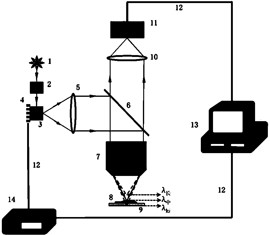
[0029] See attached figure 1 , which is a structural schematic diagram of the microstructure topography measurement device based on dispersion spectrum coding provided in this embodiment. The measuring device consists of a wide-spectrum light source 1, a beam homogeneous coupler 2, a beam deflection coupler 3, a spatial light modulator 4, a collimator beam expander lens 5, a beam splitter 6, an axial dispersion microscopic objective lens 7, An object stage 8, an imaging coupling lens 10, a snapshot multi / hyperspectral imaging detector 11, a data transmission control line 12, a computer 13 and a controller 14 are composed. The computer 13 is respectively connected to the controller 14 and the snapshot multi / hyperspectral imaging detector 11 via the data transmission control line 12; the measured element 8 is placed on the stage 9, and the measured element 8 and the spatial light modulator 4 are measuring The object-image conjugate is present at the central wavelength of the sp...


PUM


Abstract

The invention discloses a micro-structure morphology measurement method and device based on dispersion spectrum coding. According to the method and the device, a compound color sinusoidal fringe parallel light passes through an axial dispersion type optical system, then is sequentially dispersed in the axial direction and is focused on different axial depth positions in a one-to-one correspondencemode, the modulation degree of each single-color sinusoidal fringe of the axial dispersion changes along with the axial depth and reaches a maximum value near the focal plane position, so that a unique code among spectrum-modulation degree-depth required by measurement is established, and non-mechanical scanning, full-field non-contact and rapid (dynamic and even transient) high-precision measurement of the three-dimensional morphology distribution of a tested element can be realized only with multiple frames (such as three frames) of phase-shift (or single-frame) dispersion spectrum coded images.

Description

technical field [0001] The invention relates to a measurement technology of microstructure topography, in particular to a measurement device and method for microstructure topography based on dispersion spectrum coding, which belongs to the field of advanced manufacturing and detection. Background technique [0002] In semiconductor manufacturing, micro-nano optical processing, virtual reality (Virtual reality, VR), augmented reality (Augmented reality, AR) and other fields, such as microelectromechanical systems (Microelectromechanical systems, MEMS), diffractive optical elements (Diffractive optical element, DOE) have a wide range of applications. The complex microstructure formed by laser lithography, plasma etching and other processes on the surface of these components is closely related to the internal characteristics of the components such as residual stress, service life, and damage threshold. The ultra-precise detection of its microstructure morphology can provide gu...

Claims


Application Information

Patent Timeline
Patent Type & Authority Applications(China)
IPC IPC(8): G01B11/25
CPCG01B11/254
Inventor 马锁冬孙文卿曾春梅
Owner SUZHOU UNIV
Why Eureka
Try Eureka