Conductive film and conductive paste for laser etching processing
A technology of laser etching and conductivity, which is applied in the direction of conductive materials dispersed in non-conductive inorganic materials, removal of conductive materials by discharge method, printed circuit, etc., can solve the problem of longer distance and reduce ring depressions, The movement of the solvent is smooth and the effect of suppressing the failure of the disconnection
- Summary
- Abstract
- Description
- Claims
- Application Information
AI Technical Summary
Problems solved by technology
Method used
Image

Examples
Embodiment 1~3、 comparative example 1
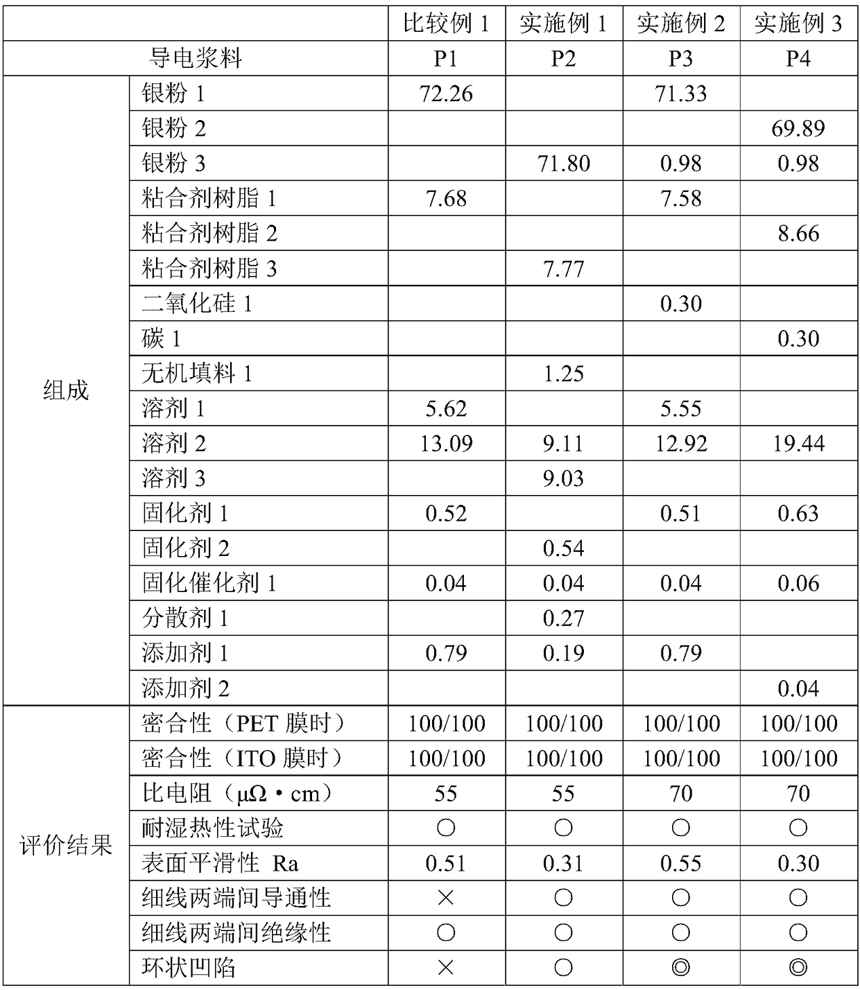
[0189] According to the mixing ratio shown in Table 1, 4 kinds of conductive pastes were adjusted. First, the binder resin is dissolved in an appropriate amount of solvent so that the solid content concentration becomes 35% by mass, and the obtained binder resin solution, silver powder 1, curing agent, curing catalyst, and remaining solvent are weighed and added. , Other additives, after pre-mixing them, pass through the cooling three-roll mixer twice to disperse. Then, a filter of 795 mesh (stainless steel mesh filter (wire diameter 16 μm, mesh 16 μm)) was attached to a slurry filter (PF320A manufactured by Protech Co., Ltd.) to filter the slurry.
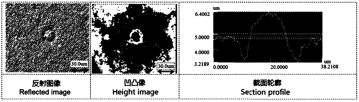
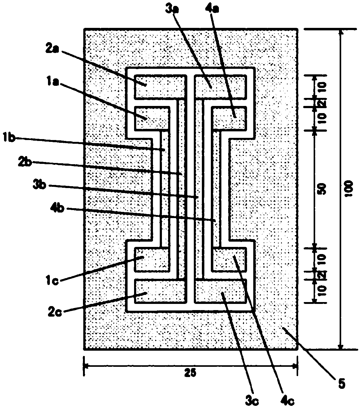
[0190] Then, the obtained conductive paste was printed in a predetermined pattern so that the dry film thickness would be 17 μm, and then dried at 120° C. for 30 minutes to obtain a conductive film. Basic physical properties were measured using the obtained conductive thin film, and then laser etching was studied. The evaluation...
Embodiment 11
[0233] According to the mixing ratio shown in Table 11, the electrically conductive paste was prepared. First, the binder resin is dissolved in an appropriate amount of solvent so that the solid content concentration becomes 35% by mass, and the obtained binder resin solution, silver powder 1, curing agent, curing catalyst, and remaining solvent are weighed and added. , Other additives, after pre-mixing them, pass through the cooling three-roll mixer twice to disperse. Then, a filter of 795 mesh (stainless steel mesh filter (wire diameter 16 μm, mesh 16 μm)) was attached to a slurry filter (PF320A manufactured by Protech Co., Ltd.) to filter the slurry. Then, after printing the obtained electroconductive paste in a predetermined pattern, it dried at 130 degreeC for 30 minutes, and obtained the electroconductive film. Basic physical properties were measured using this conductive film, and then laser etching was studied. The evaluation results are shown in Table 11.
Embodiment 12~21、 comparative example 11~13
[0235] The resin and formulation of the conductive paste were changed, and Examples 12-21 and Comparative Examples 11-13 were implemented. The formulation and evaluation results of the conductive paste are shown in Table 11. In the examples, good physical properties of the coating film can be obtained by heating in an oven at a relatively low temperature of 130° C. for 30 minutes for a short time. In addition, the evaluation after the adhesion to the ITO film and the heat-and-humidity environment test was also favorable.
[0236] Table 11
[0237]
[0238] Additionally, in Table 11,
[0239] Silver powder 1: Condensed silver powder (D50: 1.3μm)
[0240] Silver powder 2: flake silver powder (D50: 1.3μm)
[0241] Silver powder 3: Spherical silver powder (D50: 1.3μm)
[0242] Binder resin 1: PKHC manufactured by InChem (phenoxy resin, number average molecular weight 21000, Tg=89° C.)
[0243] Binder resin 2: PKHC modified product manufactured by Inchme (phenoxy resin, nu...
PUM
| Property | Measurement | Unit |
|---|---|---|
| Diameter | aaaaa | aaaaa |
| Surface roughness | aaaaa | aaaaa |
| Average film thickness | aaaaa | aaaaa |
Abstract
Description
Claims
Application Information
 - R&D
- Intellectual Property
- Life Sciences
- Materials
- Tech Scout
- Unparalleled Data Quality
- Higher Quality Content
- 60% Fewer Hallucinations
Browse by: Latest US Patents, China's latest patents, Technical Efficacy Thesaurus, Application Domain, Technology Topic, Popular Technical Reports.
© 2025 PatSnap. All rights reserved.Legal|Privacy policy|Modern Slavery Act Transparency Statement|Sitemap|About US| Contact US: help@patsnap.com