A semiconductor chip production process

A production process, semiconductor technology, applied in the direction of semiconductor/solid-state device manufacturing, electrical components, circuits, etc., can solve the problems of long changeover time, affecting processing efficiency, inconvenient wafer removal, etc., to achieve high clamping efficiency and ensure reliability Sexuality, clamping force and soft effect

Active Publication Date: 2020-12-18
日照菁英传媒科技有限公司
View PDF9 Cites 0 Cited by
  • Summary
  • Abstract
  • Description
  • Claims
  • Application Information

AI Technical Summary

Problems solved by technology

However, in this scheme, the way of clamping the wafer on the grinding disc is not convenient for taking out the wafer, thus affecting the processing efficiency; the wafer can slide in the placement groove during grinding, which affects the grinding quality of the wafer surface; when grinding wafers with different diameters The grinding disc needs to be replaced, which takes a long time to change the model and affects the processing efficiency

Method used


Image

  • A semiconductor chip production process
  • A semiconductor chip production process
  • A semiconductor chip production process

Examples


Embodiment Construction

[0031] In order to make the technical means, creative features, goals and effects achieved by the present invention easy to understand, the present invention will be further described below in conjunction with specific embodiments.

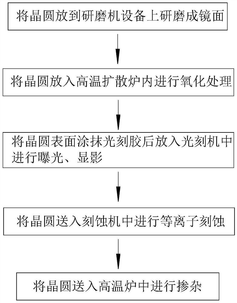
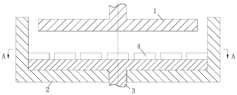
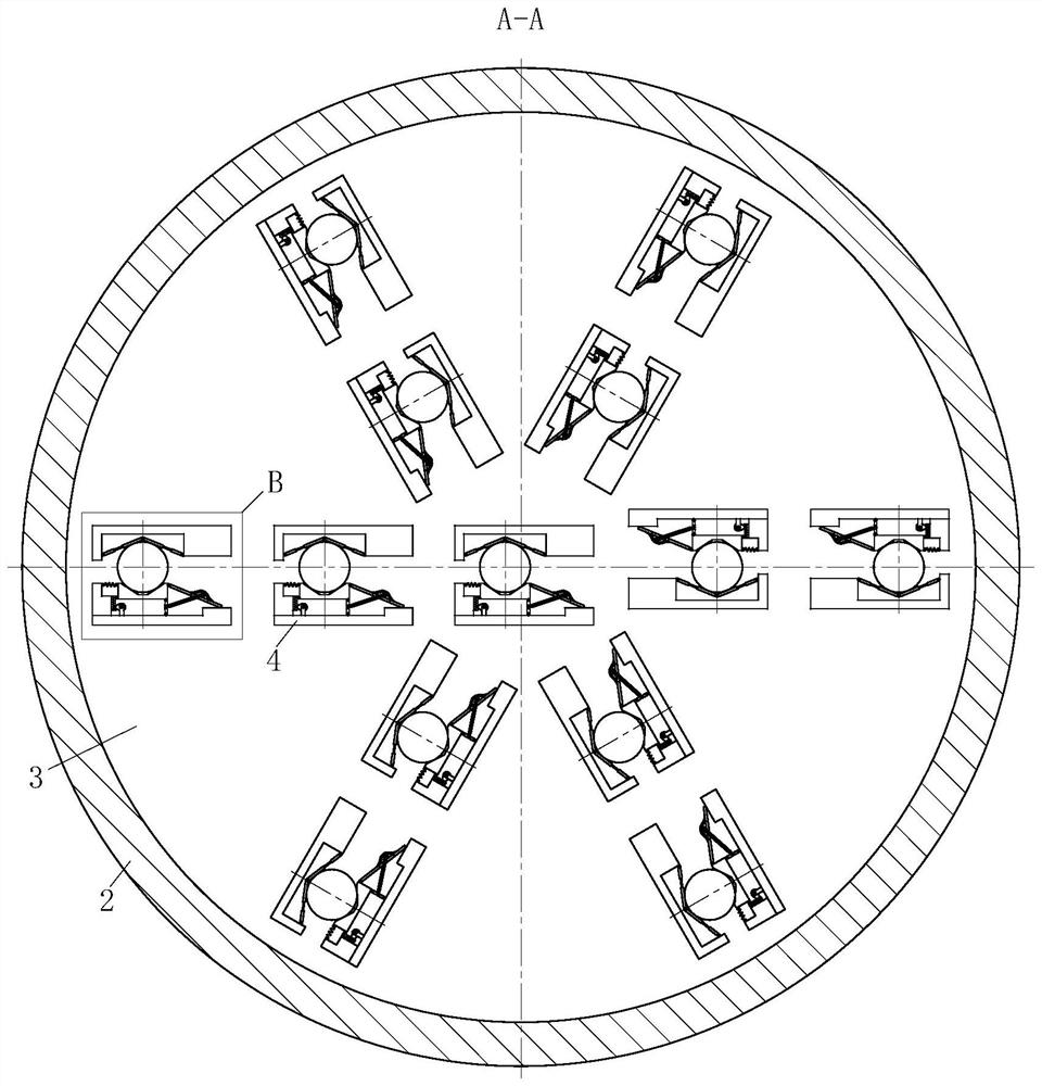
[0032] Such as Figure 1 to Figure 5 Shown, a kind of semiconductor chip production technique described in the present invention, this technique comprises the steps:

[0033] Step 1: Put the wafer on the grinding equipment and grind it into a mirror surface;

[0034] Step 2: put the wafer in step 1 into a high-temperature diffusion furnace for oxidation treatment;

[0035] Step 3: Apply photoresist on the surface of the wafer in step 2 and put it into a photolithography machine for exposure and development;

[0036] Step 4: Send the wafer in step 3 into an etching machine for plasma etching;

[0037] Step 5: Send the wafer in step 4 into a high-temperature furnace for doping;

[0038] The grinding equipment in step 1 includes a grinding sheet 1,...


PUM


Abstract

The invention belongs to the technical field of semiconductor manufacturing, in particular to a semiconductor chip production process, which comprises the following steps of: placing a wafer on a polishing device to be polished into a mirror surface; placing the wafer into a high-temperature diffusion furnace for oxidation treatment; the surface of the wafer is coated with photoresist and then putinto a photolithography machine for exposure and development; feeding the wafer into an etching machine for plasma etching; sending the wafer into a high-temperature furnace for doping; according tothe invention, a number 2 air spring is arranged under a compression spring, and the compression swing spring is compressed to swing an elastic piece, so that the wafer is clamped, and the clamping force is soft and reliable; by articulating an inclined plate at the top of the other end of the clamping block, the wafer can enter the clamping block conveniently, thereby realizing one-handed clamping of the wafer, and the clamping efficiency is higher; a mesh rack and a cam which are engaged with each other are arranged under one end of the clamping block, so that wafers with different diameterscan be grinded.

Description

technical field [0001] The invention belongs to the technical field of semiconductor manufacturing, in particular to a semiconductor chip production process. Background technique [0002] Wafer refers to the silicon chip used in the production of silicon semiconductor integrated circuits. Wafer is the carrier used in the production of integrated circuits. In general, wafers refer to single crystal silicon wafers. Wafer is the most commonly used semiconductor material. According to its diameter, it is divided into 4 inches, 5 inches, 6 inches, 8 inches and other specifications. Recently, 12 inches or even larger specifications have been developed. The larger the wafer, the more ICs that can be produced on the same wafer, which can reduce costs; but the requirements for material technology and production technology are higher, such as uniformity and so on. In wafer manufacturing, with the upgrading of process technology and the reduction of wire and gate size, photolithograph...

Claims


Application Information

Patent Timeline
Patent Type & Authority Patents(China)
IPC IPC(8): H01L21/687H01L21/304
CPCH01L21/304H01L21/68721
Inventor 王青
Owner 日照菁英传媒科技有限公司
Why Eureka
Try Eureka