Novel microwave GaN transistor with high electron mobility

A technology with high electron mobility and high GaN, applied in circuits, electrical components, semiconductor devices, etc., can solve the problems of device output power, power added efficiency, unsatisfactory transistor withstand voltage, and narrow transconductance saturation region. , to achieve the effect of reducing the influence, reducing the current collapse effect, and improving the frequency characteristics

Inactive Publication Date: 2018-11-13
XIDIAN UNIV
View PDF3 Cites 2 Cited by
  • Summary
  • Abstract
  • Description
  • Claims
  • Application Information

AI Technical Summary

Problems solved by technology

However, this type of design often leads to problems such as unsatisfactory withstand voltage of the transistor, large parasitic capacitance, and narrow transconductance saturation region, which has a great impact on important performances such as output power and power-added efficiency of the device.

Method used


Image

  • Novel microwave GaN transistor with high electron mobility

Examples


Embodiment 1

[0030] The structure of the improved GaN high electron mobility transistor is as follows.

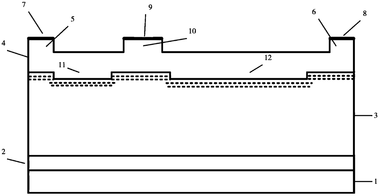
[0031] exist figure 1 Among them, the microwave gallium nitride high electron mobility transistor with high gate and multiple recessed buffer layers of the present invention has a structure from bottom to top including a semi-insulating substrate 1, an aluminum nitride nucleation layer 2, and a gallium nitride buffer layer 3 and an AlGaN barrier layer 4, a source cap layer 5 and a drain cap layer 6 on the AlGaN barrier layer, the upper surface is respectively a source electrode 7 and a drain electrode 8, between the source electrode and the drain electrode, And the gate electrode 9 is formed on the side close to the source. In the transistor, the upper surface of the high gate 10 is 5nm higher than the bottom surface, and the upper surface of the gallium nitride buffer layer directly below the source and the gate has a recess formed The left recessed region 11 has a right recessed regi...

Embodiment 2

[0037] In this embodiment, the height of the gate electrode 9 is 4 nm, the thickness of the recessed buffer layer 11 is 2 nm, and the thickness of the recessed buffer layer (12) is 2 nm.

[0038] The remaining technical solutions of this embodiment are the same as those of Embodiment 1.

Embodiment 3

[0040] In this embodiment, the height of the gate electrode 9 is 3 nm, the thickness of the left recessed region 11 is 1 nm, and the thickness of the right recessed region 12 is 1 nm.

[0041] The remaining technical solutions of this embodiment are the same as those of Embodiment 1.


PUM


Abstract

The invention provides a novel microwave GaN transistor with high electron mobility. The novel microwave GaN transistor with high electron mobility comprises a semi-insulation substrate, an aluminum nitride nucleating layer, a GaN buffer layer and AlGaN barrier layer which are arranged from bottom to top, wherein a source cap layer and a drain cap layer are arranged on the AlGaN barrier layer, a source electrode is arranged on an upper surface of the source cap layer, a drain electrode is arranged on a surface of the drain cap layer, a gate electrode is arranged between the source electrode and the drain electrode and is near to an end of the source electrode, a high gate is arranged between the source cap layer and the drain cap layer, an upper surface of the high gate is higher than a bottom surface by 5 nanometers, a left concave region is formed right below a part between the source electrode and the gate electrode and on an upper surface of the GaN buffer layer and is formed frompits, and a right concave region is formed right below a part between the drain electrode and the gate electrode and the upper surface of the GaN buffer layer and is formed from pits. By the novel microwave GaN transistor, the transconductance region of the device is improved, the saturation output power of the device is increased, and the DC characteristic and the frequency characteristic of thedevice are improved.

Description

technical field [0001] The invention relates to an electron mobility transistor, in particular to a novel microwave gallium nitride high electron mobility transistor. Background technique [0002] At the end of the 20th century, gallium nitride (GaN) has become a research hotspot in today's high-frequency and high-power devices and systems due to its large band gap, high electron saturation velocity, high breakdown voltage, and radiation resistance. Gallium Nitride High Electron Mobility Transistor (GaN HEMT), a wide bandgap semiconductor device, has the advantages of high frequency, high power density, high withstand voltage and high efficiency, so it is widely used in civil communications, Internet of Things, oil exploration, aerospace , radar systems and other civil defense have broad application prospects. [0003] In the 21st century, the development of science and technology has shown explosive growth, and the traditional GaN high electron mobility transistors can no ...

Claims


Application Information

Patent Timeline
Patent Type & Authority Applications(China)
IPC IPC(8): H01L29/778H01L29/20H01L29/06
CPCH01L29/0611H01L29/2003H01L29/778
Inventor 贾护军朱顺威胡梅赵玥阳李涛仝宜波杨银堂
Owner XIDIAN UNIV
Why Eureka
Try Eureka