All-optical diode
An all-optical diode, optical signal technology, applied in the direction of light guide, optics, optical components, etc., can solve the problems of large and complex equipment, difficult to adapt to the integration of silicon-based nanophotonic chips, and achieve high transmission contrast, simple structure, easy to integrate. Effect
- Summary
- Abstract
- Description
- Claims
- Application Information
AI Technical Summary
Problems solved by technology
Method used
Image

Examples
Embodiment Construction
[0024] In order to better understand the present invention, the content of the present invention will be further described below in conjunction with the examples and accompanying drawings, but the content of the present invention is not limited to the following examples.
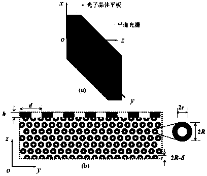
[0025] like figure 1 Shown in (a), in this embodiment, a kind of all-optical diode comprises two parts:
[0026] Photonic crystal slabs and planar gratings; where:
[0027] The photonic crystal plate is placed parallel to the plane grating;
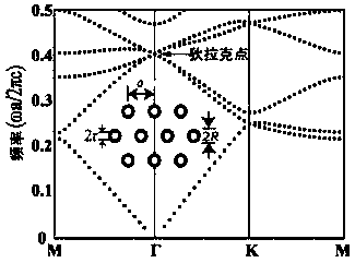
[0028] The photonic crystal plate has a triangular lattice structure composed of cylindrical shells arranged in parallel in the air, and the cross-section is as follows: figure 1 (b) shown. The distance between the cylindrical shells is the lattice constant a, and changing the lattice constant a, the inner radius r, the outer radius R and the dielectric constant ε of the cylindrical shells can change the energy band structure of the photonic crystal plate. By carefu...
PUM
 Abstract
Description
Claims
Application Information