lcos display and electronic equipment
A display and dielectric layer technology, applied in static indicators, instruments, nonlinear optics, etc., can solve problems such as unfavorable product performance, unsatisfactory low power consumption products, high power consumption of driving voltage, etc., to reduce battery effect, low Power consumption, the effect of ensuring precise voltage control
- Summary
- Abstract
- Description
- Claims
- Application Information
AI Technical Summary
Problems solved by technology
Method used
Image
Examples
Embodiment Construction
[0031] In order to make the purpose and features of the present invention more obvious and understandable, the technical solutions of the present invention will be described in detail below in conjunction with the accompanying drawings. However, the present invention can be implemented in different forms and should not be limited to the described embodiments.
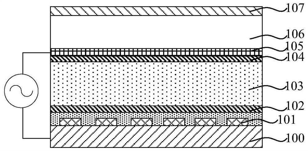
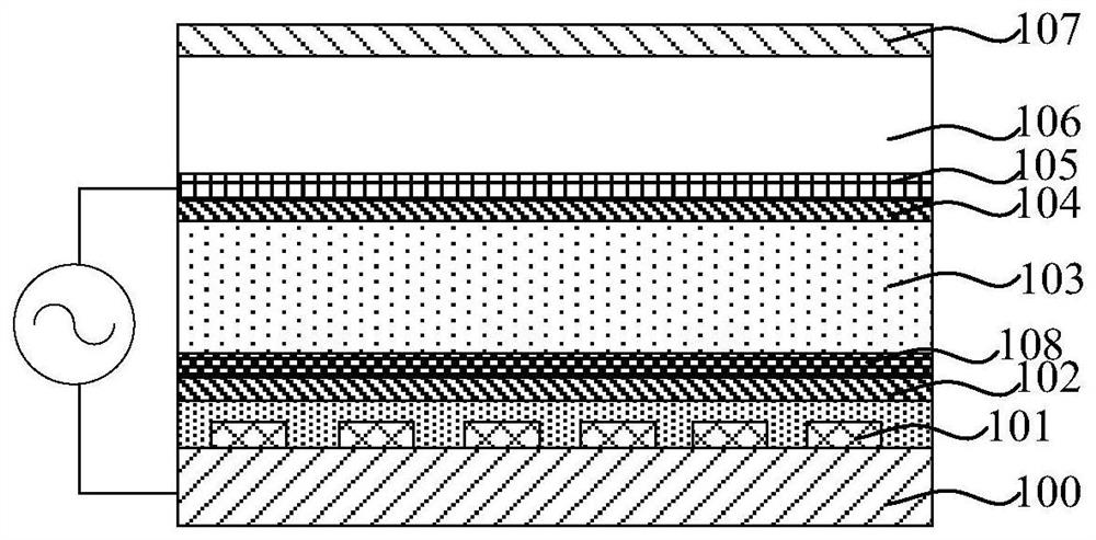
[0032] Please refer to Figure 4A to Figure 4C , the present invention provides an LCOS display, comprising a wafer substrate 300, a mirror stack 301, a pixel electrode layer 302, a first alignment layer 303, a liquid crystal layer 304, a second alignment layer 305, a transparent conductive layer 306, a transparent The cover plate 307, the anti-reflection layer 308, and the conductive via structure 300b.
[0033]Wherein, the wafer substrate 300 may be any suitable semiconductor material known to those skilled in the art, such as silicon, germanium, silicon germanium, silicon carbide, silicon-on-insulator, germanium-on-i...
PUM
 Abstract
Description
Claims
Application Information


