Epitaxial preparation method of gallium nitride LED

A technology of gallium nitride and gallium nitride layer is applied in the field of new quantum well preparation, which can solve problems such as the reduction of luminous efficiency, and achieve the effect of improving the leakage current with the increase of current density

Inactive Publication Date: 2018-11-23
贵州杰芯光电科技有限公司
View PDF4 Cites 7 Cited by
  • Summary
  • Abstract
  • Description
  • Claims
  • Application Information

AI Technical Summary

Problems solved by technology

[0004] In view of the above situation, the present invention proposes an epitaxial preparation method of gallium nitride LED, which can effectively improve the problem that the luminous efficiency decreases as the current density increases.

Method used


Image

  • Epitaxial preparation method of gallium nitride LED

Examples


Embodiment 1

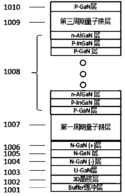
[0044] Please refer to the attached figure 1 , which shows the structural diagram of the gallium nitride-based blue LED described in this embodiment, the growth wavelength of the gallium nitride-based blue LED structure is 465nm, and the specific steps are as follows:

[0045] 1. The temperature of the MOCVD reaction chamber is raised to 560°C, the pressure is 550torr, and trimethylgallium (160ml / min) and NH3 are introduced at the same time for 3.5 minutes, and the reaction occurs to form a 28nm GaN buffer layer 1001 layer;

[0046] 2. Then set the temperature to 1060°C for 9 minutes and drop the pressure to 500torr to make the buffer layer react and form nuclei islands; maintain the temperature at 1060°C and the pressure to 500torr, and inject trimethylgallium (200ml / min) and ammonia gas (30l / min) for a total of 30 minutes, so that the small islands of crystal nuclei grow laterally, and finally the islands merge with the islands; a two-dimensional crystal layer 1002 is forme...


PUM

PropertyMeasurementUnit
thicknessaaaaaaaaaa
thicknessaaaaaaaaaa
thicknessaaaaaaaaaa

Abstract

The invention discloses an epitaxial preparation method of a gallium nitride LED. The method comprises the following steps of growing a gallium nitride buffer layer on a sapphire substrate; annealingthe gallium nitride buffer layer shape to form at least one crystal nucleus island-buffer layer; and transversely growing the gallium nitride layer on the basis of the crystal nuclear island until allthe crystal nuclear islands are connected with each other, so as to form an integral two-dimensional crystal layer-3D crystal nucleus layer. According to the preparation method, a buffer insertion layer is grown in the middle of an active region. The buffer insertion layer is formed by alternately laminating a first sub-layer, a second sub-layer and a third sub-layer. The first sub-layer is madeof P-type gallium nitride, the second sub-layer is made of P-type indium gallium nitrogen, and the third sub-layer is made of N-type aluminum gallium nitrogen. According to the technical scheme, the functions of electronic deceleration and uniform expansion are achieved through consumption, blocking and emission effects. The problem of leakage current of positive conduction is solved, and the problem that the light emitting efficiency of the conventional gallium nitride LED epitaxial structure is lowered along with the increasing of the current density is solved.

Description

【Technical field】 [0001] The patent of the present invention relates to an epitaxial preparation method of gallium nitride light-emitting diodes, in particular to a novel quantum well preparation method 【Background technique】 [0002] Semiconductor light-emitting diodes have the characteristics of high luminous efficiency, long life, small size, rich colors, etc., and are widely used. Semiconductor light-emitting diodes emit light by radiative recombination of electrons and holes in the active region sandwiched between the n-type doped region and the p-type doped region. The difference in the mobility of electrons and holes is an important reason affecting the luminous efficiency. Generally, the mobility of electrons is more than 10 times that of holes. The difference in mobility causes a large number of electrons to cross the active region and enter the p-type doped region to recombine with holes, which affects the luminous efficiency. [0003] In the traditional GaN lig...

Claims


Application Information

Patent Timeline
Patent Type & Authority Applications(China)
IPC IPC(8): H01L33/00H01L33/06H01L33/14H01L33/32
CPCH01L33/007H01L33/06H01L33/14H01L33/32
Inventor 尹宝堂李敏贤林淇乐
Owner 贵州杰芯光电科技有限公司
Why Eureka
Try Eureka