Pressure and temperature sensor based on wafer bonding and manufacturing method thereof

A technology of temperature sensor and manufacturing method, applied in the direction of instruments, measuring instrument components, measuring devices, etc.

Inactive Publication Date: 2020-11-10
ZHEJIANG UNIV
View PDF5 Cites 0 Cited by
  • Summary
  • Abstract
  • Description
  • Claims
  • Application Information

AI Technical Summary

Problems solved by technology

[0003] Wafer bonding is often used to make MEMS pressure sensors, but there are few methods based on wafer bonding for simultaneous time pressure and temperature sensing

Method used


Image

  • Pressure and temperature sensor based on wafer bonding and manufacturing method thereof
  • Pressure and temperature sensor based on wafer bonding and manufacturing method thereof
  • Pressure and temperature sensor based on wafer bonding and manufacturing method thereof

Examples


Embodiment Construction

[0039] The manufacturing method of the pressure and temperature sensor based on wafer bonding of the present invention comprises the following steps:

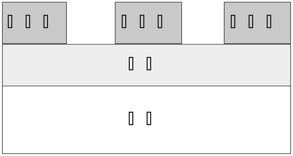
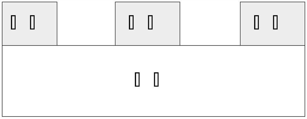
[0040] 1) making a metal layer on a silicon wafer; the metal layer includes a central circular area and an annular area surrounding the circular area and having a gap with the circular area;

[0041] 2) filled with polymer and piezoelectric particles;

[0042] Spin-coating polymer in the gap between the circular area of ​​the metal layer and the annular area; filling the circular area of ​​the metal layer with piezoelectric particles;

[0043] 3) bonding;

[0044] Align and bond the structures obtained in the two steps 2) up and down;

[0045] 4) Drill holes and fill them with metal.

[0046] Punch holes on the upper and lower silicon wafers of the structure obtained in step 3), and the punching position is located in the circular area of ​​the center of the metal layer, and the depth of the punching reaches to the exposed m...


PUM

PropertyMeasurementUnit
thicknessaaaaaaaaaa
diameteraaaaaaaaaa
thicknessaaaaaaaaaa

Abstract

The invention discloses a manufacturing method of pressure and temperature sensor based on wafer bonding. The method comprises the following steps: 1) a metal layer is manufactured on a silicon wafer,and the metal layer comprises a circular region located in the center and an annular region which surrounds the circular region and is provided with a gap with the circular region; 2) a polymer and piezoelectric particles are filled; 3) the structures obtained in the two steps are aligned and bonded; 4) punching is carried out and the metal is filled. The pressure and temperature sensor based onwafer bonding can achieve low-temperature, low-voltage and rapid bonding of the metal wafers together, meanwhile, the electrical connection in the vertical direction is realized, and the resistance value in the vertical direction is sensitive to pressure and temperature.

Description

technical field [0001] The invention belongs to the field of micro-electromechanical systems, and specifically designs a pressure and temperature sensor based on wafer bonding and a manufacturing method thereof. Background technique [0002] MEMS sensors are a class of sensors that have been greatly used recently. Compared with all kinds of traditional sensors in the past, it has the advantages of small size, light weight, low energy consumption, small inertia, high reliability, short response time, and excellent mechanical and electrical properties. In addition, it is precisely because MEMS sensors can use a series of integrated circuit design techniques and manufacturing processes, which facilitates its high-precision, low-cost mass production, and greatly reduces production costs. MEMS sensors have a very broad application space in many fields such as water conservancy and hydropower, railway transportation, intelligent buildings, production automation, aerospace, milita...

Claims


Application Information

Patent Timeline
Patent Type & Authority Patents(China)
IPC IPC(8): G01D21/02G01D11/00
CPCG01D11/00G01D21/02
Inventor 朱智源夏克泉徐志伟
Owner ZHEJIANG UNIV
Why Eureka
Try Eureka