Method for achieving silicon through hole laminated chip interconnection

A through-silicon via and chip technology, applied in semiconductor devices, electrical components, circuits, etc., can solve problems such as low reliability of solder joints, long bonding time, and affecting joint performance, and achieve excellent comprehensive mechanical properties and shorten bonding time. The effect of time, excellent bonding effect

Inactive Publication Date: 2014-08-06
HARBIN INST OF TECH
View PDF3 Cites 17 Cited by
  • Summary
  • Abstract
  • Description
  • Claims
  • Application Information

AI Technical Summary

Problems solved by technology

Bonding at temperatures above 260°C will affect the performance of sensitive chips in the package
During the bonding process, the wafer or chip warpage is caused by the mismatch of the thermal expansion coefficient of each layer of material, which affects the accuracy in high-density, narrow-pitch packaging interconnection
[0004] (2) High bonding pressure
The chip is prone to cracks under the action of high bonding pressure or fixture force, causing damage to the wafer or chip
[0005] (3) Solder joint reliability is low
Chip interconnection solder joints in stacked packages are usually only 3~6μm, and the interior of the solder joints is almost entirely composed of intermetallic compounds, which are brittle substances in the interconnection joints, which seriously affect the performance of the joints
In addition, electromigration will drive the continued growth of intermetallic compounds, causing thermal mismatch of various parts in the package to cause failure
[0006] (4) Long bonding time
The heating time in the wafer-level bonding process is as long as tens of minutes or even several hours, which is not in line with the characteristics of high-efficiency electronic manufacturing

Method used


Image

  • Method for achieving silicon through hole laminated chip interconnection
  • Method for achieving silicon through hole laminated chip interconnection
  • Method for achieving silicon through hole laminated chip interconnection

Examples


specific Embodiment approach 1

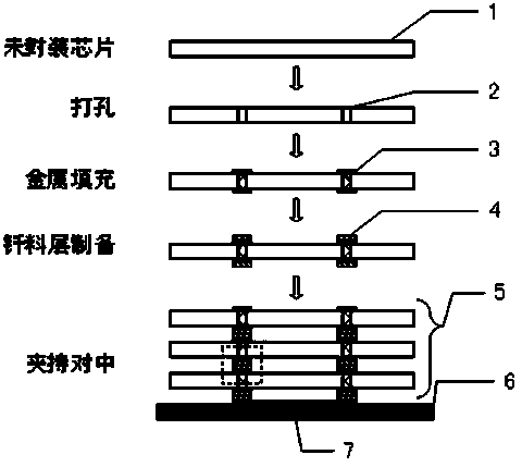
[0026] Specific implementation mode one: as Figure 1~5 As shown, this embodiment provides a method for realizing TSV all-intermetallic solder joint bonding by current Joule heat. In this embodiment, strong current bonding of multi-layer stacked TSV chips is carried out according to the following steps:

[0027] (1) Drilling: Drilling the chip 1, the specific method is: forming a through hole 2 in the silicon crystal by etching or laser drilling, and then using plasma enhanced chemical vapor deposition (PECVD), physical vapor deposition (PVD) ) or Metal Organic Compound Chemical Vapor Deposition (MOCVD) to sequentially deposit metal adhesion layer Ti or Ta, barrier layer TiN or TaN / A seed layer (Cu, Ag or Ag) to obtain a through-silicon via chip packaged on a stack, and the thickness of the chip is less than 100 μm;

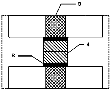
[0028] (2) Filling of conductive metal and flattening of pads: use electroplating to fill the through-hole 2 conductive metal 3 of the laminated package thr...

Embodiment approach 2

[0033] Specific implementation method two: such as Image 6 As shown, this embodiment provides a method for realizing all-intermetallic compound solder joint bonding in a current-ultrasonic composite field, and the steps are as follows:

[0034] (1)~(4) Repeat steps (1)~(4) in the specific implementation method 1;

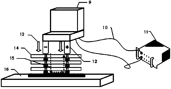
[0035] (5) An ultrasonic device is integrated in the processing platform 16 so that the ultrasonic contact 19 is flush with the surface of the processing platform 16 . First turn on the double-pulse narrow-gap parallel resistance welding equipment 9 to start the DC power switch 11, and when the electrode contacts 12 press the stacked chips 5 under pneumatic action, the ultrasonic power supply 20 is quickly turned on. The current intensity is appropriately reduced to the range of 0.6~1.0KA, the pressure 13 of the electrode contact 12 needs to be appropriately increased (3~10N), the chip is placed and moved, the bonding time is 90ms~1000ms, the ultrasonic frequency ...

Embodiment approach 3

[0037] Specific implementation method three: such as Figure 7As shown, this embodiment provides a low temperature current Joule heating to realize TSV all-intermetallic compound solder joint bonding, and the steps are as follows:

[0038] (1)~(4) Repeat steps (1)~(4) in the specific implementation method 1;

[0039] (5) Place the heating plate device 21 on the processing platform 16 . Turn on the power supply 22 of the heating plate 30s in advance to preheat the device to be processed, and the preheating temperature is 50-150°C. Then turn on the double-pulse narrow-gap parallel resistance welding equipment 9, start the DC power switch 11, and the electrode contact 12 will press the stacked chip 5 under pneumatic action, and form a closed circuit in the solder joint 18-pad 8-substrate copper wiring 7 The current of the loop is 15; the control current intensity is 0.6KA~1.2KA, the welding time is 90ms~1500ms, and the pressure 13 of the electrode contact is 2~8N. The process ...


PUM

PropertyMeasurementUnit
electrical conductivityaaaaaaaaaa
thicknessaaaaaaaaaa

Abstract

The invention discloses a method for achieving silicon through hole laminated chip interconnection. The method is used for achieving bonding among multiple layers of stacked silicon through hole chips through the following steps of punching, filling of conductive metal, preparing of a solder layer, clamping and centering, bonding and forming of finished products, wherein in the bonding process, a current joule heat auxiliary bonding technology is adopted for achieving silicon through hole three-dimensional interconnection welding spot bonding. According to the method for achieving three-dimensional packaging and bonding with the assistance of joule heat, under the low temperature and even the normal temperature, fast bonding of full intermetallic compound welding spots can be achieved, and heat damage to a chip is effectively reduced. Under the action of oriented currents, intermetallic compounds in the welding spots are grown preferably and rapidly in an oriented mode, high electrical conductivity and the good comprehensive mechanical property of the welding spots are achieved, and the reliability of the bonding spots is effectively improved. A parallel electrode resistance welding platform is adopted, a hot plate and an ultrasound device are easily integrated, the better bonding effect can be achieved, and the bonding time is shortened.

Description

technical field [0001] The invention belongs to the technical field of electronic manufacturing, and relates to a new method for quickly realizing the interconnection of stacked chips with high reliability through-silicon vias (TSVs) under the conditions of relatively low preheating temperature and normal temperature. Background technique [0002] Through Silicon Via (TSV) stack packaging technology realizes the interconnection between chips by making vertical through holes between chips and between wafers. Because of its multi-functional chip, reduced signal delay, reduced power consumption, and reduced packaging volume, it is widely favored by academics and industries. It is the core of today's high-density three-dimensional chip packaging technology and is regarded as the successor. The fourth generation of packaging technology after wire bonding, tape bonding and flip chip. The TSV technology process mainly includes: preparation and filling of through holes, wafer thinn...

Claims


Application Information

Patent Timeline
Patent Type & Authority Applications(China)
IPC IPC(8): H01L21/768H01L21/603H01L21/607
CPCH01L24/82H01L21/76898H01L2021/60007H01L2224/82H01L2224/16145H01L2224/16225
Inventor 田艳红刘宝磊孔令超王春青
Owner HARBIN INST OF TECH
Why Eureka
Try Eureka