Integrated optical waveguide electric field sensor and electric field measurement system utilizing same
An integrated optical waveguide and sensor technology, applied in the direction of electrostatic field measurement, etc., can solve the problems that cannot meet the requirements of transient electric field measurement, and achieve the effect of ensuring miniaturization
- Summary
- Abstract
- Description
- Claims
- Application Information
AI Technical Summary
Problems solved by technology
Method used
Image

Examples
Embodiment 1
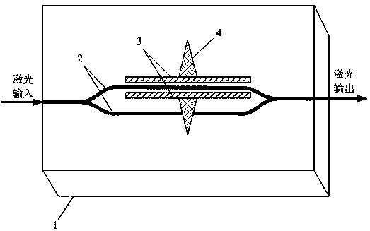
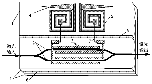
[0029] Embodiment 1: as Figure 1-4 As shown, an integrated optical waveguide field sensor includes a lithium niobate chip 1, a modulation electrode 3, a dipole antenna 4, a planar spiral inductor 5, and an ultraviolet curing glue 6;
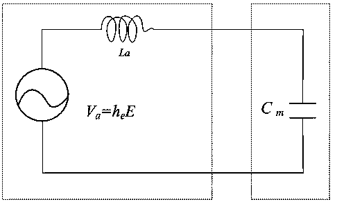
[0030] in one piece x cut y An integrated optical waveguide Mach-Zehnder interferometer 2 composed of an input Y-shaped optical waveguide, a straight waveguide arm, and an output Y-shaped optical waveguide is manufactured on the surface of the lithium niobate wafer 1, and the integrated optical waveguide Mach-Zehnder interferometer 2 Modulating electrodes 3 are made on both sides of the two straight waveguide arms or on both sides of one of the straight waveguide arms; a dipole antenna 4 and a planar spiral inductor 5 are made on the surface of another lithium niobate wafer 1, and one end of the planar spiral inductor 5 is directly connected to the The dipole antenna 4 is connected, and the other end is connected to the modulation electrode 3 ...
Embodiment 2
[0048] Embodiment 2: as Figure 5 As shown, the difference between this embodiment and embodiment 1 is that the structure of the modulation electrode 3 is different. Two parallel electrode sheets and a parallel electrode arranged between the two straight waveguide arms of the integrated optical waveguide Mach-Zehnder interferometer 2, two parallel electrodes arranged outside the two straight waveguide arms of the integrated optical waveguide Mach-Zehnder interferometer 2 The plates are connected together through the connecting electrode sheet and then connected to the planar spiral inductor 5 on the left side through the connecting wire 7, and a piece of parallel electrode arranged between the two straight waveguide arms of the integrated optical waveguide Mach-Zehnder interferometer 2 is connected to the wire through the connecting electrode sheet 7 is connected with the planar spiral inductor 5 on the right side.
Embodiment 3
[0049] Embodiment 3: as Image 6 As shown, the difference between this embodiment and Embodiment 1 is that the structure of the modulation electrode 3 is different. In this embodiment: specifically, the modulation electrode 3 includes one of the integrated optical waveguide Mach-Zehnder interferometers 2 The two parallel electrode sheets on both sides of the straight waveguide arm are arranged on the inside of the straight waveguide arm of the integrated optical waveguide Mach-Zehnder interferometer 2. The parallel electrode sheet is connected to the plane spiral inductor 5 on the right after connecting the electrode sheet to the connecting wire 7. The parallel electrode sheet outside the straight waveguide arm of the integrated optical waveguide Mach-Zehnder interferometer 2 is connected to the planar spiral inductor 5 on the left after connecting the electrode sheet connection wire 7 .
[0050] figure 2 , Figure 5 , Image 6 The characteristic of the modulation electrod...
PUM
 Abstract
Description
Claims
Application Information
 - R&D
- Intellectual Property
- Life Sciences
- Materials
- Tech Scout
- Unparalleled Data Quality
- Higher Quality Content
- 60% Fewer Hallucinations
Browse by: Latest US Patents, China's latest patents, Technical Efficacy Thesaurus, Application Domain, Technology Topic, Popular Technical Reports.
© 2025 PatSnap. All rights reserved.Legal|Privacy policy|Modern Slavery Act Transparency Statement|Sitemap|About US| Contact US: help@patsnap.com