

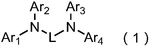
Organic light-emitting device
A technology of organic light-emitting devices and light-emitting layers, which is applied in the manufacture of electric solid-state devices, semiconductor devices, semiconductor/solid-state devices, etc., and can solve problems such as carrier injection imbalance, low luminous efficiency of light-emitting devices, and recombination region offset
- Summary
- Abstract
- Description
- Claims
- Application Information
AI Technical Summary
Problems solved by technology
Method used
Image


Examples
Embodiment 1
[0122] Embodiment 1: the synthesis of compound 1-A6
[0123]
[0124] Synthesis of intermediate a1-6
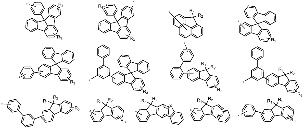
[0125] Tri-tert-butylphosphine (4.4 mL of a 1.0 M solution in toluene, 1.48 g, 0.05 mmol), palladium acetate (0.4 g, 1.83 mmol) and sodium tert-butoxide (22.8 g, 238 mmol) were added to N,N'- A solution of diphenylbenzidine (61.5 g, 183 mmol) and 3-bromo-9,9-dimethylfluorene (49.9 g, 183 mmol) in degassed toluene (1 L), and the mixture was heated at reflux for 2 Hour. The reaction mixture was cooled to room temperature, diluted with toluene and filtered through celite. The filtrate was diluted with water and extracted with toluene, and the combined organic phases were evaporated under vacuum. The residue was filtered through silica gel and recrystallized. Intermediate a1-6 (77.3 g, 80% yield) was obtained.
[0126] Mass Spectrum m / z: 528.63 (calculated: 528.68). Theoretical element content (%)C 39 h 32 N 2 : C, 88.60; H, 6.10; N, 5.30 The measured element content ...
Embodiment 2
[0139] Embodiment 2: the synthesis of compound 1-A17
[0140]
[0141] Replace N,N'-diphenylbenzidine in Example 1 with equimolar N,N'-diphenylbenzidinediamine, and 3-bromo-9,9-dimethylfluorene with equimolar 2-bromo-dibenzofuran, other steps are the same as the synthesis of Example 1 to obtain the target product compound 1-A17. Mass Spectrum m / z: 816.93 (calculated: 816.98). Theoretical element content (%)C 61 h 40 N 2O: C, 89.68; H, 4.93; N, 3.43; O, 1.96 Measured element content (%): C, 89.67; H, 4.94; N, 3.41; O, 1.98. The above results confirmed that the obtained product was the target product.
Embodiment 3
[0142] Embodiment 3: the synthesis of compound 1-A38
[0143]
[0144] The N,N'-diphenylbenzidine in Example 1 was replaced with an equimolar compound A, and the other steps were the same as in Example 1 to obtain the target compound 1-A38. Mass Spectrum m / z: 883.26 (calculated: 883.13). Theoretical element content (%)C 67 h 50 N 2 : C, 91.12; H, 5.71; N, 3.17 Measured element content (%): C, 91.13; H, 5.72; N, 3.15. The above results confirmed that the obtained product was the target product.
PUM
 Abstract
Description
Claims
Application Information