Semiconductor structures and methods of forming them

A semiconductor and formation layer technology, which is applied in semiconductor/solid-state device manufacturing, grinding machine tools, manufacturing tools, etc., can solve the problems that the electrical properties of semiconductor structures need to be improved, and achieve the effects of improving grinding quality, corrosion, and electrical properties

Active Publication Date: 2021-09-07
SEMICON MFG INT (SHANGHAI) CORP +1
View PDF8 Cites 0 Cited by
  • Summary
  • Abstract
  • Description
  • Claims
  • Application Information

AI Technical Summary

Problems solved by technology

[0004] However, even if a material with a lower resistance value is selected for the contact hole plug, the electrical performance of the semiconductor structure still needs to be improved.

Method used


Image

  • Semiconductor structures and methods of forming them
  • Semiconductor structures and methods of forming them
  • Semiconductor structures and methods of forming them

Examples


Embodiment Construction

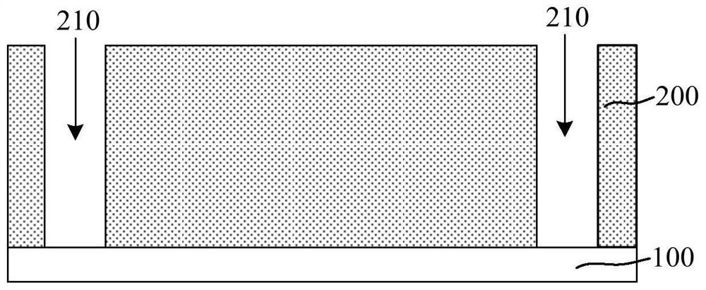
[0031] It can be seen from the background art that even if the contact hole plug is made of a material with a lower resistance value, the electrical performance of the semiconductor structure still needs to be improved. Analysis performance still needs to be improved because:

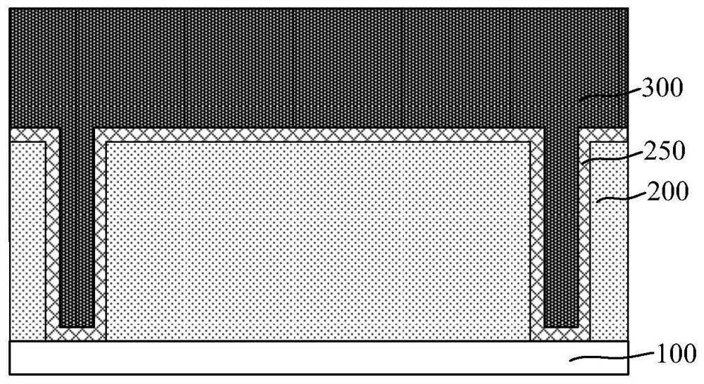
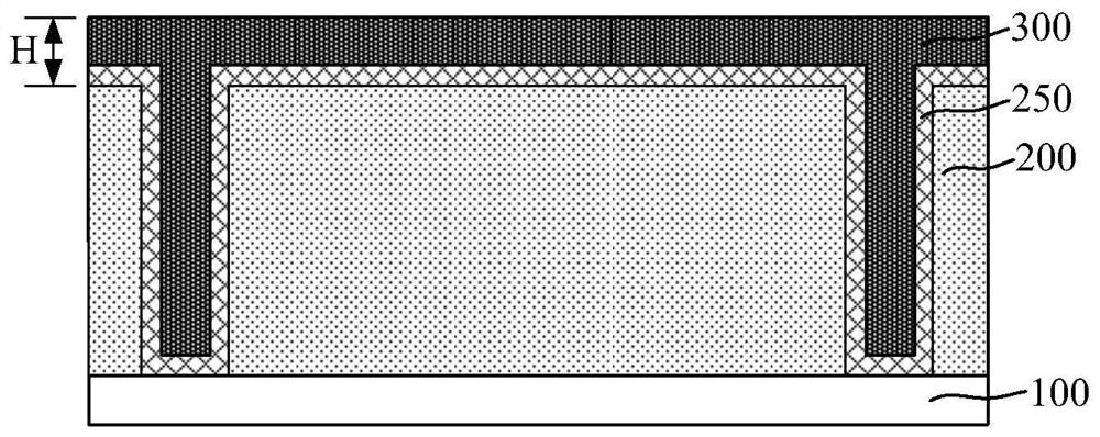
[0032] Since the cobalt material has a small resistance value and a good filling performance (Gap Filling), currently in the field of semiconductor manufacturing, the commonly used material for the contact hole plug (CT) is cobalt, which is beneficial to reduce the RC delay.

[0033] When a chemical and mechanical polishing (CMP) process is used to planarize the cobalt layer, the solution used in the cleaning operation and the transmission operation in the chemical mechanical polishing process is deionized water (DIW). The material is prone to corrosion (Corrosion) when exposed to deionized water; in addition, when the chemical mechanical polishing process uses an acidic grinding liquid, the acidic grin...


PUM

PropertyMeasurementUnit
relative permittivityaaaaaaaaaa

Abstract

A semiconductor structure and a forming method thereof, the forming method comprising: forming a cobalt layer; planarizing the cobalt layer by using a chemical mechanical polishing process, wherein the polishing liquid used in the chemical mechanical polishing process is a weakly alkaline polishing liquid; Wherein, the solutions used in the cleaning operation and the conveying operation in the chemical mechanical polishing process are weakly alkaline solutions. The present invention adopts weakly alkaline grinding liquid, and the solutions used in the cleaning operation and conveying operation in the chemical mechanical grinding process are all weakly alkaline solutions, compared with the use of acid grinding liquid and deionized water for the cleaning operation And the solution of the transmission operation, the present invention can improve the corrosion problem of the cobalt layer, thereby improving the grinding quality of the cobalt layer, and further improving the electrical performance of the semiconductor structure.

Description

technical field [0001] The invention relates to the field of semiconductor manufacturing, in particular to a semiconductor structure and a forming method thereof. Background technique [0002] In a semiconductor device, reducing the RC delay (Resistance Dapacitance Delay) can improve the performance of the semiconductor device. With the development of semiconductor technology and the advancement of technology nodes, the functions of devices are becoming more and more powerful, the integration of devices is getting higher and higher, and the feature size (Critical Dimension, CD) of devices is getting smaller and smaller. Correspondingly, the RC is further reduced. Delay has become one of the important measures to improve the performance of semiconductor devices. [0003] An interconnection structure of a semiconductor device includes contact hole plugs. At present, in order to reduce the RC delay, the material used for the contact hole plug is usually a material with a smal...

Claims


Application Information

Patent Timeline
Patent Type & Authority Patents(China)
IPC IPC(8): H01L21/306B24B37/11B24B37/00
CPCB24B37/0056B24B37/11H01L21/30625
Inventor 蒋莉
Owner SEMICON MFG INT (SHANGHAI) CORP
Why Eureka
Try Eureka