Manufacturing method of diode having ladder type structure

A manufacturing method, ladder-shaped technology, applied in the field of diodes, can solve problems such as glass damage, high grain glass height, and low yield

Inactive Publication Date: 2018-12-07
YEA SHIN TECH
View PDF8 Cites 0 Cited by
  • Summary
  • Abstract
  • Description
  • Claims
  • Application Information

AI Technical Summary

Problems solved by technology

[0005] However, if figure 1 As shown in the PN diode grain 10, the protective layer 104, which acts as an insulating protection during the sintering process, after sintering, in order to completely protect the insulation of the grain, the structure formed by it will be higher than the P-type semiconductor layer 103; therefore , in the subsequent heat dissipation packaging process, in order to match the structure of the protective layer 104 protruding from the periphery of the PN diode crystal grain 10, the heat sink 105 on the P-type semiconductor layer 103 must have a convex structure to be completely flat on the P-type semiconductor layer 103. semiconductor layer 103, such as figure 2 As shown; because the protruding structure of the protective layer 104 is different, the heat sink 105 for heat dissipation cannot be completely attached to the P-type semiconductor layer 103 when it is packaged, causing the problem of uneven heat dissipation, and such The structure is also easy to cause the crystal glass structure to be too high, which makes it easy to cause damage to the glass during packaging, resulting in a decrease in the yield and affecting the production efficiency of the diode crystal

Method used


Image

  • Manufacturing method of diode having ladder type structure
  • Manufacturing method of diode having ladder type structure
  • Manufacturing method of diode having ladder type structure

Examples


Embodiment Construction

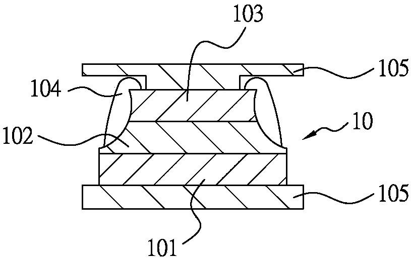
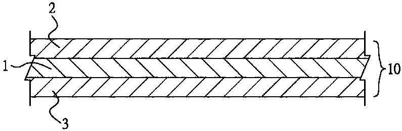
[0027] see Figure 3 to Figure 6 As shown, it is a schematic diagram of the manufacturing process structure of the present invention. like image 3 As shown, the diode die structure of the present invention mainly includes an N-type semiconductor layer 1. In this embodiment, the N-type semiconductor layer 1 is an N-type crystal (N-type wafer), and the N-type semiconductor layer 1 is stacked on one side. A P-type semiconductor layer 2, an N+-type semiconductor layer 3 is attached to the other side of the N-type semiconductor layer 1, the P-type semiconductor layer 2 and the N+-type semiconductor layer 3 are made of boron paper and phosphorous paper respectively in the process It is attached to both sides of the N-type semiconductor layer 1, and then the P-type semiconductor layer 2 and the N+-type semiconductor layer 3 are respectively formed after a burn-off process, a pre-deposition process, a soaking and separation process, a wet oxidation process and a diffusion process. ...


PUM


Abstract

The invention provides a manufacturing method of a diode having a ladder type structure. The diode crystal grain structure mainly comprises an N-type semiconductor layer, wherein a P-type semiconductor layer is stacked on one side of the N-type semiconductor layer, and an N+ type semiconductor layer is attached to the other side of the N-type semiconductor layer; a trench is formed in a peripheryof the P-type semiconductor layer; an insulating protective layer is arranged at the periphery of the N-type semiconductor layer and in the trench of the P-type semiconductor layer, and the top surface of the insulating protective layer is not higher than the top surface of the P-type semiconductor layer; and through the design of the trench of the P-type semiconductor layer, the height of the insulating protective layer is reduced so as to ensure improvement of the excellent rate of the subsequent packaging process and improvement of the overall efficiency of the diode.

Description

technical field [0001] The present invention relates to a diode, in particular to a method for manufacturing a diode with a stepped structure. Background technique [0002] The rectifier diode is a separate component in the industry. The main purpose of the rectifier diode is to rectify and suppress abnormal signals. The so-called rectification refers to the ability to convert alternating current into direct current, and the suppression of abnormal signals refers to the input signal exceeding the limit range. Part of it is removed to maintain the stability of the input signal as a protection circuit. The rectifier diode is used in the fields of semiconductors, communications and consumer electronics, and is one of the indispensable electronic components. [0003] The structure of the diode die is currently known, such as figure 1 As shown in the schematic diagram of the known die structure, the known diode die is a PN diode die 10, the diode die structure includes an N+ typ...

Claims


Application Information

Patent Timeline
IPC IPC(8): H01L21/329
CPCH01L29/6609
Inventor 彭工及萧上智张靖奇黄承扬
Owner YEA SHIN TECH
Why Eureka
Try Eureka