Solar cell and preparation method thereof, battery piece based on solar cell and photovoltaic module

A technology of solar cells and photovoltaic modules, applied in photovoltaic power generation, electrical components, circuits, etc., can solve the problems of sliced ​​battery power output attenuation, single battery unit, device performance attenuation, etc., to avoid edge leakage and short circuit, and avoid performance attenuation , to avoid the attenuation effect

Inactive Publication Date: 2018-12-07
LONGI SOLAR TECH (TAIZHOU) CO LTD
View PDF6 Cites 8 Cited by
  • Summary
  • Abstract
  • Description
  • Claims
  • Application Information

AI Technical Summary

Problems solved by technology

However, the sliced ​​batteries used in prior art 1 and prior art 2 are all complete single battery units, that is, the sliced ​​batteries used in prior art 1 and prior art 2 contain only one pn junction
In the cutting process, the original complete pn junction is cut into several pn junction units, and the pn junction is the core structure of the solar cell, once it is destroyed, it will inevitably cause the attenuation of device performance, so prior art one and prior art Second, it will still cause the power output of the sliced ​​battery to attenuate, and the yield rate is low

Method used


Image

  • Solar cell and preparation method thereof, battery piece based on solar cell and photovoltaic module
  • Solar cell and preparation method thereof, battery piece based on solar cell and photovoltaic module
  • Solar cell and preparation method thereof, battery piece based on solar cell and photovoltaic module

Examples


preparation example Construction

[0059] The preparation method of solar cell provided by the invention, its process is as follows:

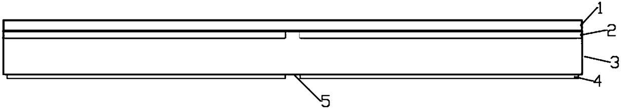
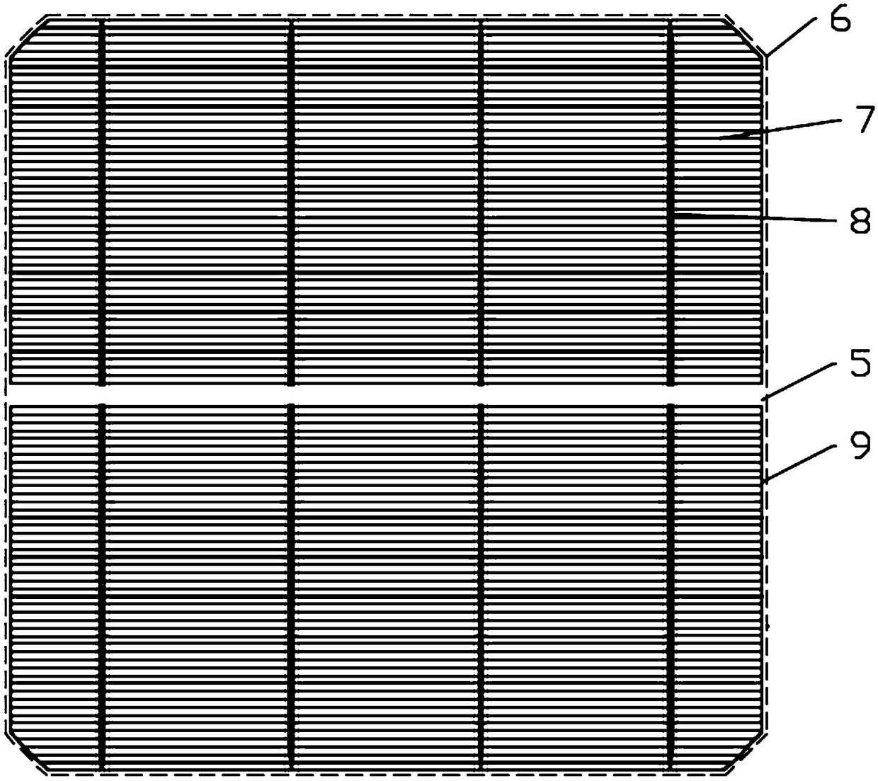
[0060] Prepare several independent emitters 2 on one surface of the silicon substrate 3 with a textured light-trapping structure, and there is a preset distance between the edges of adjacent emitters 2;

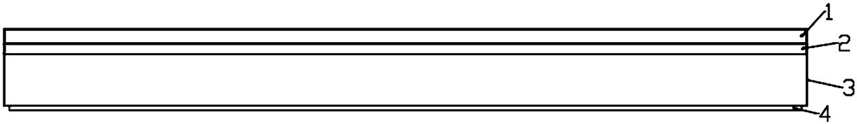
[0061] Prepare a passivation layer 1 on the surface of the silicon substrate prepared with the emitter 2;

[0062] Prepare the electrode pattern again, when preparing the electrode pattern, prepare an independent front electrode pattern on the surface of the passivation layer 1 corresponding to each emitter 2; on the other surface of the silicon substrate 3, correspond to each emitter 2 area to prepare independent back electrode patterns.

[0063] As a preferred embodiment of the present invention, the silicon substrate 3 forms a textured light-trapping structure by chemical etching.

[0064] As a preferred embodiment of the present invention, the electrode pattern is prepare...

Embodiment 1

[0071] The process of preparing solar cells in this embodiment is as follows:

[0072] (1) Texturing: Put the P-type monocrystalline silicon wafer of M2 size in potassium hydroxide alkali solution for anisotropic etching to form a pyramidal light-trapping structure;

[0073] (2) Diffusion: the P-type monocrystalline silicon wafer after texturing is placed in a tubular diffusion furnace and heated in POCl 3 High-temperature diffusion in a gas atmosphere, after the diffusion is completed, a complete pn junction will be formed;

[0074] (3) Etching: Coat the surface of the diffused P-type single crystal silicon wafer with a layer of paraffin, and leave a blank area with a width of about 4 mm in the middle of the P-type single crystal silicon wafer without paraffin. The single crystal silicon wafer is etched in a chain cleaning tank to remove the side junction and back junction formed during the diffusion process and the pn junction in the paraffin-free area on the surface;

[0...

Embodiment 2

[0079] The process of preparing solar cells in this embodiment is as follows:

[0080] (1) Texturing: Put the P-type monocrystalline silicon wafer of M2 size in sodium hydroxide alkali solution for anisotropic etching to form a pyramidal light-trapping structure;

[0081] (2) Diffusion: the P-type monocrystalline silicon wafer after texturing is placed in a tubular diffusion furnace and heated in POCl 3 High-temperature diffusion in a gas atmosphere, after the diffusion is completed, a complete pn junction will be formed;

[0082] (3) Etching: Coat the surface of the diffused P-type single crystal silicon wafer with a layer of paraffin, and leave a blank area with a width of about 4 mm in the middle of the P-type single crystal silicon wafer without paraffin. The single crystal silicon wafer is etched in a chain cleaning tank to remove the side junction and back junction formed during the diffusion process and the pn junction in the paraffin-free area on the surface;

[0083...


PUM


Abstract

The present invention discloses a solar cell and preparation method thereof, a battery piece based on a solar cell and a photovoltaic module. Transmitting electrodes on a silicon substrate of a solarcell are a plurality of independent transmitting electrodes, and preset distances are arranged between edges of the adjacent transmitting electrodes; the positive electrode patterns and the negative electrode patterns of a dye-sensitized solar cell are a plurality of independent electrode patterns, and each transmitting electrode corresponds to one independent positive electrode pattern and one independent negative electrode pattern up and down. When the solar cell is sliced, the portion between the edges of the adjacent transmitting electrodes perform cutting for the solar cell to prevent thesolar cell from damaging the pn junction in the slicing process to cause performance degradation of the solar cell and avoid edge leakage and short circuit because the electrode residual slurry afterslicing and the metal powder in the slicing process pollute a notch; and moreover, the notch stress is small to reduce the battery piece fragmenting or subfissure caused by stress releasing and improve the slicing yield and module reliability.

Description

technical field [0001] The invention belongs to the technical field of crystalline silicon solar cells, and in particular relates to a solar cell, a preparation method thereof, and a solar cell and a photovoltaic module based thereon. Background technique [0002] A solar cell is a photoelectric device that uses the photovoltaic effect to directly convert light energy into electrical energy. According to the matrix material used to manufacture solar cells, it can generally be divided into silicon-based solar cells, compound solar cells, thin-film solar cells, organic solar cells, nano-solar cells, and the like. At present, silicon-based solar cell technology is the most mature and has been commercially produced on a large scale, accounting for more than 85% of the solar cell market. [0003] A general crystalline silicon solar cell consists of a silicon substrate, an emitter, a light-trapping structure on the emitter surface, a passivation anti-reflection structure on the e...

Claims


Application Information

Patent Timeline
Patent Type & Authority Applications(China)
IPC IPC(8): H01L31/0224H01L31/0352H01L31/068H01L31/18
CPCH01L31/022433H01L31/022441H01L31/035281H01L31/068H01L31/0682H01L31/1804Y02E10/542Y02E10/547Y02P70/50
Inventor 王建波陈传科李鹏朱琛吕俊
Owner LONGI SOLAR TECH (TAIZHOU) CO LTD
Why Eureka
Try Eureka