A double-sided three-dimensional stacked packaging structure and packaging method

A three-dimensional stacking and packaging structure technology, applied in the direction of semiconductor/solid-state device components, semiconductor devices, electrical components, etc., can solve problems such as component warpage, and achieve the effect of reducing the occupied area and improving the utilization rate

Inactive Publication Date: 2018-12-14
NAT CENT FOR ADVANCED PACKAGING
View PDF5 Cites 10 Cited by
  • Summary
  • Abstract
  • Description
  • Claims
  • Application Information

AI Technical Summary

Problems solved by technology

[0003] The double-sided three-dimensional stack packaging structure and method provided by the present invention overcome the problem of element warpage caused by the mismatch of thermal expansion of one side in the prior art

Method used


Image

  • A double-sided three-dimensional stacked packaging structure and packaging method
  • A double-sided three-dimensional stacked packaging structure and packaging method
  • A double-sided three-dimensional stacked packaging structure and packaging method

Examples


Embodiment 1

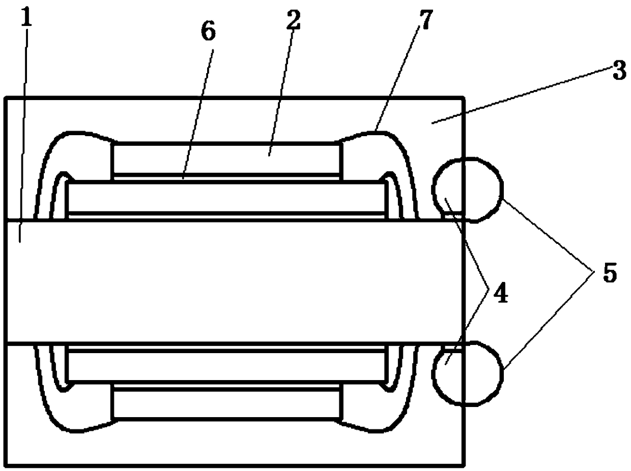
[0033] An embodiment of the present invention provides a double-sided three-dimensional stack package structure, such as figure 1 As shown, the double-sided three-dimensional stack package structure includes: a substrate 1 and a chip 2, at least one layer of chips 2 are respectively stacked on the first surface and the second surface of the substrate 1, and the chip 2 is electrically interconnected with the substrate 1; The chip 2 is encapsulated by a plastic encapsulation material 3 to form a package structure.

[0034] In the embodiment of the present invention, the substrate 1 is provided with wiring, and the chip 2 is electrically interconnected with the substrate 1 through the bonding wire 7. The bonding wire 7 is a gold wire with a diameter of 20um. The bonding wire is selected from a gold wire because it has a large electrical conductivity. , corrosion resistance, good toughness advantages. But it is not limited thereto. In other embodiments, the welding wire 7 can be ...

Embodiment 2

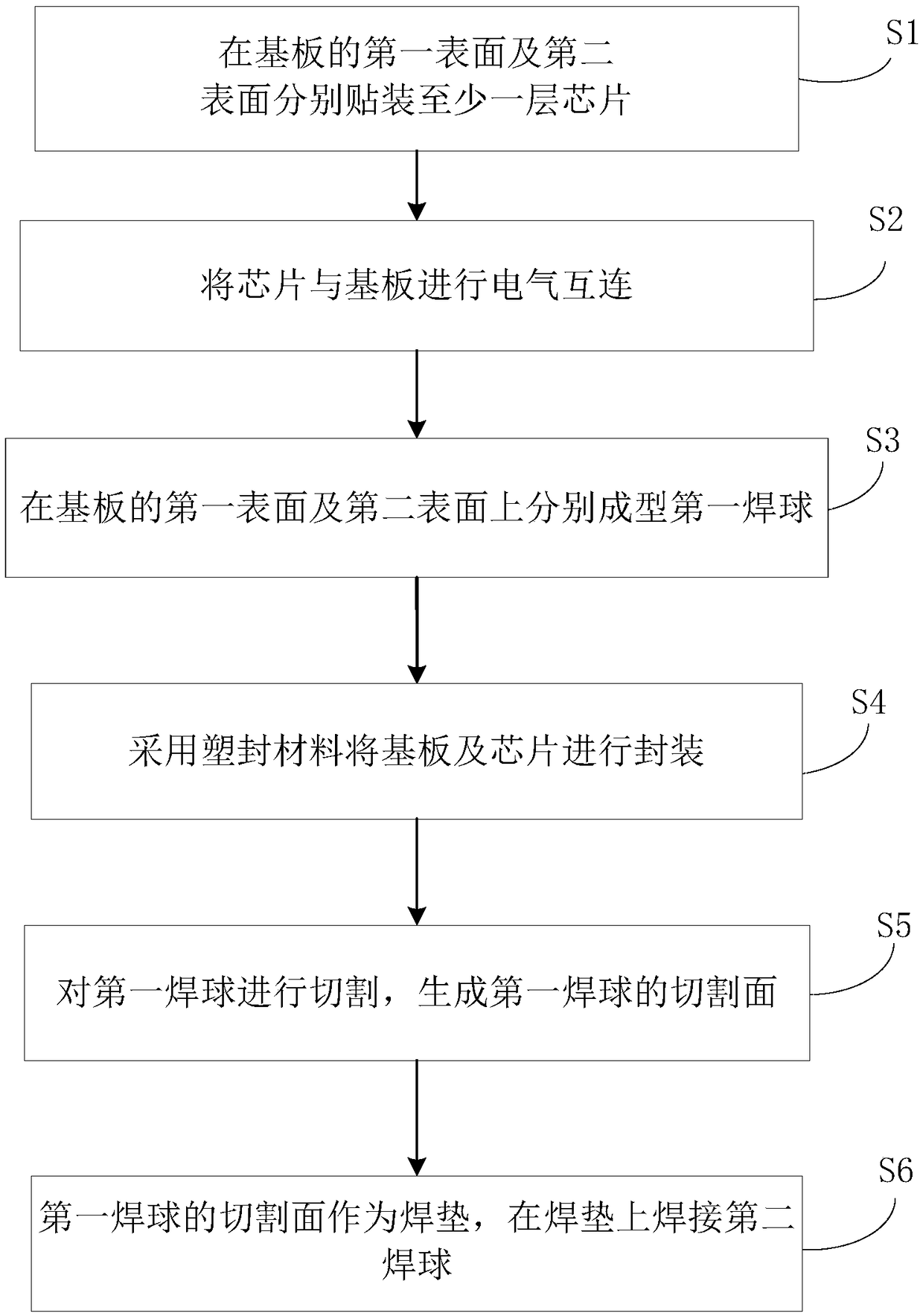
[0040] An embodiment of the present invention provides a double-sided three-dimensional stack packaging method, such as figure 2 As shown, the double-sided three-dimensional stack packaging method includes the following steps:

[0041] Step S1: mounting at least one layer of chips on the first surface and the second surface of the substrate respectively.

[0042] In a preferred embodiment, the same number of chips are mounted symmetrically on the first surface and the second surface of the substrate, so as to reduce or avoid the problem of warpage after plastic packaging caused by mismatching thermal expansion systems of different materials.

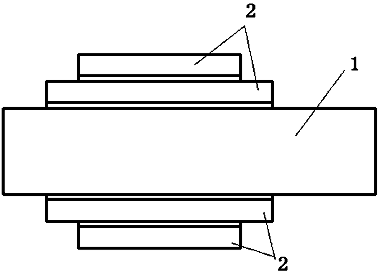
[0043] In the embodiment of the present invention, such as image 3 As shown, two layers of chips 2 are mounted symmetrically on the first surface and the second surface of the substrate 1 . But it is not limited thereto. In other embodiments, different numbers of chips can be mounted on the first surface and the second surface of the...


PUM


Abstract

The invention discloses a double-sided three-dimensional stacked packaging structure and a packaging method, The method comprises: At least one chip is respectively mounted on the first surface and the second surface of the substrate, the chip is electrically interconnected with the substrate, the substrate and the chip are encapsulated with a plastic encapsulating material, solder balls are respectively formed on the first surface and the second surface of the substrate, the solder balls are cut to form a cutting surface, and the cutting surface is used as a solder pad for secondary implantation. The invention adopts double-sided plastic sealing process, chips and solder balls mounted on both sides of the substrate are protected by plastic packaging, The invention solves the component warping problem caused by the mismatch of one-sided thermal expansion, realizes the system integration of larger capacity or function through double-sided chip stacking, and reduces the occupied area ofthe board-level assembled circuit board through the side interconnection technology, and improves the utilization ratio of the final board-level assembled circuit board.

Description

technical field [0001] The invention relates to the technical field of semiconductor packaging, in particular to a double-sided three-dimensional stack packaging structure and a packaging method. Background technique [0002] The traditional packaging process is to stack the chips in multiple layers on the front of the substrate, and realize the electrical interconnection of chips to chips and chips to the substrate by wire bonding or flip chip, and then carry out plastic packaging for protection. The back of the substrate generally realizes the final soldering of the components to the PCB board level by planting BGA solder balls. The problem to be faced is that the packaging components are: a combination of substrates, chips, glue, plastic packaging materials and other materials, and the thermal expansion system of the materials does not match. The problem of warping after plastic packaging is caused, and the more chips are stacked, the thicker the plastic packaging is, and...

Claims


Application Information

Patent Timeline
Patent Type & Authority Applications(China)
IPC IPC(8): H01L23/31H01L23/535H01L21/56
CPCH01L23/535H01L21/56H01L23/3114H01L2224/32145H01L2224/32225H01L2224/73265H01L2224/48091H01L2924/00014
Inventor 金国庆
Owner NAT CENT FOR ADVANCED PACKAGING
Why Eureka
Try Eureka