A GaN field effect transistor have a P buried lay connected to a source and a drain field plate

A technology of drain field plate and source electrode, applied in the direction of semiconductor devices, electrical components, circuits, etc., can solve the problems of large leakage current, damage to device reliability, and deterioration of device performance, to improve withstand voltage, reduce leakage current, increase Pressure-resistant effect

Active Publication Date: 2018-12-14
HANGZHOU DIANZI UNIV
View PDF5 Cites 8 Cited by
  • Summary
  • Abstract
  • Description
  • Claims
  • Application Information

AI Technical Summary

Problems solved by technology

The physical properties of the wide bandgap GaN material and the Si substrate are very different, such as the lattice constant and the thermal expansion coefficient do not match, which makes the heteroepitaxial growth of the GaN buffer layer on the silicon wafer inevitably produce lattice mismatch and Dislocations, while the stresses caused by the lattice constant and thermal expansion coefficient mismatch in the structure can also damage the reliability of the device, and finally in the GaN buffer layer can generate up to 10 10 cm -3 Defects
Due to the doping of impurities and point defects, the grown GaN is basically n-type doped, and the background leakage current is relatively large, which will easily lead to the deterioration of the performance of the device, which may cause premature breakdown of the device.

Method used


Image

  • A GaN field effect transistor have a P buried lay connected to a source and a drain field plate
  • A GaN field effect transistor have a P buried lay connected to a source and a drain field plate
  • A GaN field effect transistor have a P buried lay connected to a source and a drain field plate

Examples


Embodiment Construction

[0015] In order to make the purpose, technical solution and advantages of the present invention clearer, the present invention will be described in detail below in conjunction with the accompanying drawings.

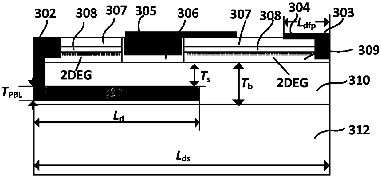
[0016] The invention is a voltage-resistant AlGaN / GaN insulated gate field-effect transistor with a source-connected P-type buried layer and a drain field plate, such as image 3 As shown, it includes a source electrode 302, a drain electrode 303, a drain field plate 304, a gate electrode 305, a gate dielectric layer 306, a passivation layer 307, a barrier layer 308, a channel layer 309, a low-concentration trap-doped buffer layer 310, It is connected to the source electrode with a P-type buried layer 311 and a high-concentration trap-doped buffer layer 312 .

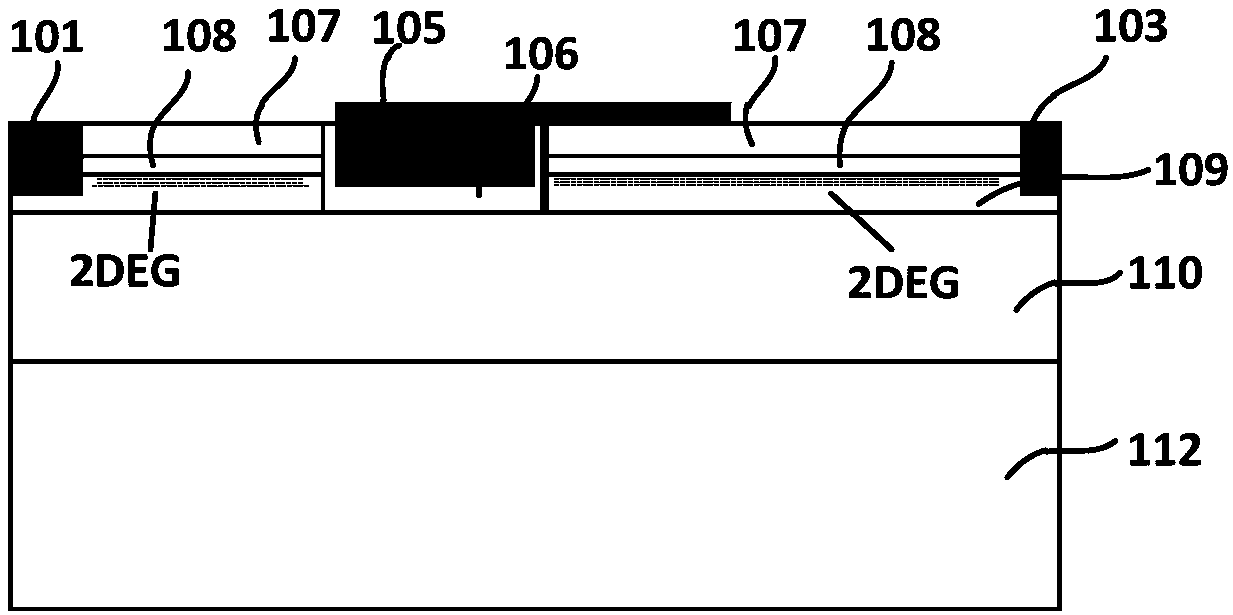
[0017] Such as figure 1 Shown is a schematic structural diagram of a traditional gate field plate insulated gate AlGaN / GaN field effect transistor, which can be used as one of the comparison devices of the presen...


PUM


Abstract

A GaN field effect transistor comprise a gate electrode, a source region, a gate dielectric layer, a passivation lay, a barrier layer, a channel layer, a low-concentration trap dope buffer layer, a high-concentration trap doping buffer layer, a P-type buried layer connected to that source electrode, and a drain field plate. A P-type bury layer connected with that source electrode is located in a low-concentration trap doping buffer lay, and the drain field plate is located on the passivation layer and the gate electrode is extended. When the transistor of the invention operates at the off-state high voltage, the P-type buried layer is connected with the drain electrode so as to sufficiently deplete the carriers in the channel and the buffer layer, thereby reducing the leakage current in the buffer layer and modulating the electric field distribution between the gate and the drain at the same time. On the basis of the P-type buried layer connected to the drain, the drain field plate canfurther modulate the electric field at the drain end, and finally the withstand voltage characteristic of the device is obviously improved compared with the traditional pure gate field plate AlGaN/GaN insulated gate field effect transistor.

Description

technical field [0001] The invention relates to a semiconductor power device for high withstand voltage, in particular to a voltage-resistant AlGaN / GaN insulated gate field-effect transistor with a source-connected P-type buried layer and a drain field plate. Background technique [0002] With the continuous development of the world economy, energy consumption continues to increase, non-renewable energy oil reserves are less and less, and the awareness of environmental protection crises in various countries is gradually increasing. In order to reduce the waste of electric energy in power conversion and control of power electronic systems The energy conversion efficiency of the enhancement mode power transistor, the core component in the power electronic system, has been receiving much attention. However, in the power electronic systems of various countries, the enhanced power switching devices used are still mainly Si-based MOSFETs and IGBTs. After years of development, the...

Claims


Application Information

Patent Timeline
Patent Type & Authority Applications(China)
IPC IPC(8): H01L29/778H01L29/40
CPCH01L29/402H01L29/7783
Inventor 王颖罗昕于成浩曹菲
Owner HANGZHOU DIANZI UNIV
Why Eureka
Try Eureka