A preparation method of a light emitting diode epitaxial wafer and a light emitting diode epitaxial wafer thereof

A technology of light-emitting diodes and epitaxial wafers, which is applied in semiconductor/solid-state device manufacturing, electrical components, circuits, etc., can solve the problems of bound carrier migration, low LED luminous efficiency, etc., to increase the number of holes, reduce series resistance, The effect of lowering the forward voltage

Active Publication Date: 2018-12-25
HC SEMITEK ZHEJIANG CO LTD
View PDF4 Cites 5 Cited by
  • Summary
  • Abstract
  • Description
  • Claims
  • Application Information

AI Technical Summary

Problems solved by technology

[0006] The embodiment of the present invention provides a method for preparing a light-emitting diode epitaxial wafer and the light-emitting diode epitaxial wafer, which can solve the problem in the prior art that high-concentration defects in the contact layer will bind the migration of carriers and cause low luminous efficiency of the LED. question

Method used


Image

  • A preparation method of a light emitting diode epitaxial wafer and a light emitting diode epitaxial wafer thereof
  • A preparation method of a light emitting diode epitaxial wafer and a light emitting diode epitaxial wafer thereof

Examples


Embodiment Construction

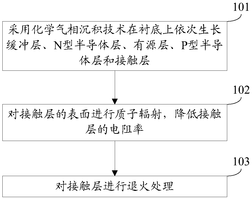
[0025] In order to make the object, technical solution and advantages of the present invention clearer, the implementation manner of the present invention will be further described in detail below in conjunction with the accompanying drawings.

[0026] The embodiment of the present invention provides a method for preparing a light-emitting diode epitaxial wafer, figure 1 For the flow chart of the preparation method of the light-emitting diode epitaxial wafer provided by the embodiment of the present invention, see figure 1 , the preparation method comprises:

[0027] Step 101: growing a buffer layer, an N-type semiconductor layer, an active layer, a P-type semiconductor layer and a contact layer sequentially on the substrate by chemical vapor deposition technology.

[0028] Specifically, this step 101 may include:

[0029] Controlling the temperature to 400°C to 600°C (preferably 500°C), the pressure to 400torr to 600torr (preferably 500torr), and growing a buffer layer with...


PUM


Abstract

The invention discloses a preparation method of a light emitting diode epitaxial wafer and a light emitting diode epitaxial wafer thereof, belonging to the field of semiconductor technology. A manufacture method comprises sequentially growing a buffer layer, an N-type semiconductor layer, an active layer, a P-type semiconductor lay and a contact layer on a substrate by a chemical vapor depositiontechnique; applying proton radiation to the surface of the contact layer to reduce the resistivity of the contact layer. The present invention provides a method for preparing a contact layer by protonirradiation on the surface of the contact layer, changing the microstructure of contact layer crystal, affecting the shape and number of defects in the contact layer and decreasing the resistivity ofthe contact layer can improve the carrier mobility of the contact layer, facilitate the hole migration of the P-type semiconductor layer into the active layer, increase the number of holes in the active layer, further increase the radiative recombination luminescence of the holes in the active layer, and finally improve the luminescence efficiency of the LED. Moreover, the resistivity of the contact layer is reduced, and the series resistance of the epitaxial wafer can be reduced, and finally the forward voltage of the LED can be reduced.

Description

technical field [0001] The invention relates to the technical field of semiconductors, in particular to a method for preparing a light-emitting diode epitaxial wafer and the light-emitting diode epitaxial wafer. Background technique [0002] A light-emitting diode (English: Light Emitting Diode, referred to as: LED) is a semiconductor electronic component that can emit light. LED has attracted wide attention due to its advantages of energy saving, environmental protection, high reliability, and long service life. For civil lighting, luminous efficiency and service life are the main criteria, so increasing the luminous efficiency of LEDs and improving the antistatic ability of LEDs is particularly critical for the wide application of LEDs. [0003] Epitaxial wafers are the primary products in the LED manufacturing process. The existing LED epitaxial wafer includes a substrate, a buffer layer, an N-type semiconductor layer, an active layer and a P-type semiconductor layer, a...

Claims


Application Information

Patent Timeline
Patent Type & Authority Applications(China)
IPC IPC(8): H01L33/14H01L33/12H01L21/268H01L33/00
CPCH01L21/268H01L33/007H01L33/12H01L33/14
Inventor 郭炳磊王群葛永晖吕蒙普胡加辉李鹏
Owner HC SEMITEK ZHEJIANG CO LTD
Why Eureka
Try Eureka