An accumulation type DMOS device

An accumulation type, device technology, used in semiconductor devices, electrical components, diodes, etc., can solve problems such as large static power consumption, and achieve the effects of high reverse withstand voltage, good reverse recovery characteristics, and low on-resistance

Inactive Publication Date: 2018-12-28
UNIV OF ELECTRONICS SCI & TECH OF CHINA
View PDF5 Cites 3 Cited by
  • Summary
  • Abstract
  • Description
  • Claims
  • Application Information

AI Technical Summary

Problems solved by technology

However, the accumulation power DMOS is always on when no voltage is applied to the gate, and it is a normally-on device, so it has a large static power consumption.

Method used


Image

  • An accumulation type DMOS device
  • An accumulation type DMOS device

Examples


Embodiment 1

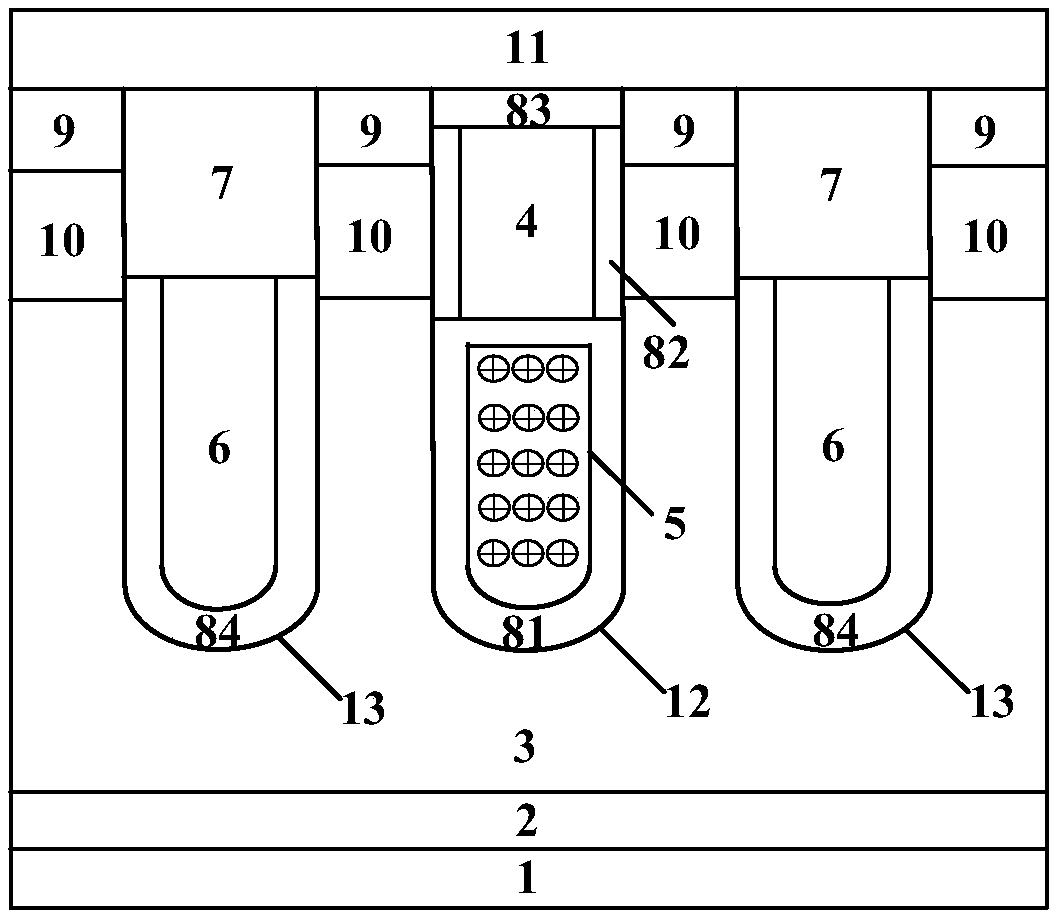
[0017] An accumulation DMOS device, comprising a metallized drain 1, an N+ substrate 2, an N-drift region 3, and a metallized source 11 stacked sequentially from bottom to top, and the upper layer of the N-drift region 3 has an N- Type lightly doped region 10, the N-type lightly doped region 10 has an N+ heavily doped region 9 directly above, the upper surface of the N+ heavily doped region 9 is in contact with the metallized source 11, the N- The inside of the drift region 3 also has a first trench 12 and a second trench 13, and the first trench 12 runs through the N+ heavily doped region 9 and the N-type The lightly doped region 10 then extends into the N-drift region 3, the second trenches 13 are located on both sides of the first trench, and the second trenches 13 vertically and downwardly penetrate the N+ The heavily doped region 9 and the N-type lightly doped region 10 then extend into the N-drift region 3, the first trench has a polysilicon gate electrode 4 and a positi...

Embodiment 2

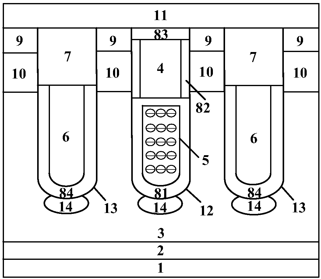
[0031] Such as figure 2As shown, the structure of this embodiment is based on Embodiment 1, and a P-type buried layer 14 is implanted at the bottom of the polysilicon field plate 6 and the positive charge region 5 . In this way, when the device is reversely blocked, the P-type buried layer 14 and the N-drift region 3 form a lateral electric field, which further increases the breakdown voltage of the device.


PUM


Abstract

The invention provides an accumulation type DMOS device, comprising a metallized drain electrode, an N + substrate, an N-drift region and a metallized source which are successively stacked from bottom to top. The upper layer of the N-drift region has an N-type light doped region, and an N + heavily doped region is located directly above the N-type light doped region. The N-drift region is also provided with a first trench and a second trench inside, wherein the first trench is provided with a polysilicon gate electrode and a positive charge region, the polysilicon gate electrode and the metallization source electrode are isolated by a second dielectric layer, and the positive charge region is positioned directly below the polysilicon gate electrode. The depth of the lower surface of the N-type light doped region is smaller than that of the lower surface of the polycrystalline silicon gate electrode. The invention solves the problem that the conventional accumulated power DMOS is a normally-on device. The invention is not only a normally-off device, but also has the advantages of low threshold voltage, small on resistance, high reverse withstand voltage, good reverse recovery characteristic of the body diode and no parasitic transistor.

Description

technical field [0001] The invention relates to power semiconductor technology, in particular to an accumulation type DMOS device. Background technique [0002] Power DMOS plays an important role in the field of power conversion because of its advantages such as fast switching speed, low loss, high input impedance, low driving power, and good frequency characteristics. Under high current, power DMOS has a negative temperature coefficient, there is no secondary breakdown problem of bipolar power devices, and the safe operating area is relatively large. The development of power DMOS devices is based on the advantages of MOS devices, and strives to improve withstand voltage and reduce losses. [0003] Initially, DMOS was considered as an ideal switching device because of its high input impedance and simple driving. However, the internal resistance between source and drain limits the power handling capability of DMOS. The on-resistance of power DMOS includes: source region re...

Claims


Application Information

Patent Timeline
Patent Type & Authority Applications(China)
IPC IPC(8): H01L29/78H01L29/40H01L29/423H01L29/06H01L29/36
CPCH01L29/0684H01L29/36H01L29/402H01L29/4236H01L29/7806H01L29/7813
Inventor 李泽宏杨梦琦蒲小庆赵阳任敏张金平高巍张波
Owner UNIV OF ELECTRONICS SCI & TECH OF CHINA
Why Eureka
Try Eureka