An epitaxial wafer and a growth method for improving the antistatic ability of a gallium nitride-based LED light emitting diode

A light-emitting diode, gallium nitride-based technology, applied in circuits, electrical components, semiconductor devices, etc., can solve surface defects, affect chip anti-static problems, etc., and achieve the effect of optimizing design, improving anti-static ability, and uniform density distribution

Inactive Publication Date: 2018-12-28
HUAIAN AUCKSUN OPTOELECTRONICS TECHNOLOGY CO LTD
View PDF17 Cites 7 Cited by
  • Summary
  • Abstract
  • Description
  • Claims
  • Application Information

AI Technical Summary

Problems solved by technology

Due to the different lattice constants of the two materials, it is easy to produce polarization effects and cause dislocation defects. If the defects are not effectively controlled, the line dislocations passing through the GaN / InGaN quantum well barrier region will cause a large number of surface defects, forming Leakage channels, which in turn affect the ability of the chip to withstand antistatic

Method used


Image

  • An epitaxial wafer and a growth method for improving the antistatic ability of a gallium nitride-based LED light emitting diode

Examples


Embodiment 1

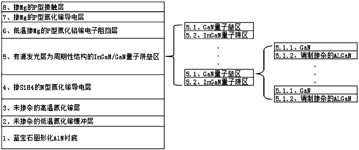
[0042] An epitaxial wafer growth method for improving the antistatic ability of gallium nitride-based LED light-emitting diodes, comprising the following process steps:

[0043] Step 1: After cleaning the sapphire patterned ALN substrate, put it on the graphite disk in the MOCVD chamber, and bake it at about 1040°C for 11 minutes;

[0044] Step 2: Cool down to 525°C and grow a low-temperature GaN layer with a thickness of 27nm under a pressure of 500mbar;

[0045] Step 3: Raise the temperature to 1110°C and grow a high-temperature GaN layer with a thickness of 2200nm under a pressure of 750mbar;

[0046] Step 4: growing a SiH4-doped n-type high-temperature GaN layer with a thickness of 2700 nm at a temperature of 1065° C. and a pressure of 600 mbar;

[0047] Step 5: At a temperature of 825°C and a pressure of 300mbar, a layer of 2nm GaN is grown, and then a layer of 2nm modulated doped AlGaN is grown, and the two are used as a superlattice unit structure, which is grown alter...


PUM


Abstract

An epitaxial wafer and a growth method for improving the antistatic ability of a gallium nitride-based LED light emitting diode are provided, wherein the epitaxial wafer structure sequentially comprises a sapphire patterned AlN substrate, an undoped low-temperature gallium nitride buffer layer, an undoped high-temperature gallium nitride layer, an SiH4 doped N-type gallium nitride conductive layer, an active light emitting layer, a low-temperature Mg doped P-type aluminum gallium nitride electron blocking layer, a Mg doped P-type gallium nitride conductive layer and a Mg doped P-type contact layer from bottom to top. The invention proposes that the quantum barrier layer adopts a modulation doped GaN / AlGaN superlattice structure, which can effectively guide the impulse current, so that thepulse current is generated in the two-dimensional electron gas of GaN / AlGaN structure; the density distribution of the pulse current is more uniform because of conduction in the transverse direction,so that the possibility of LED chip breakdown is greatly reduced; the epitaxial wafer growth method is provided for effectively improving the antistatic ability of GaN-based light emitting diodes.

Description

technical field [0001] The invention belongs to the technical field of design and application of gallium nitride-based LED epitaxial wafers, and relates to an epitaxial wafer and a growth method for improving the antistatic ability of gallium nitride-based LED light-emitting diodes. Background technique [0002] Gallium nitride (GaN) is a wide bandgap material with high resistivity. The electrostatic charge generated during the production and transportation of GaN-based LED chips is not easy to disappear, and it can generate a high electrostatic voltage when accumulated to a certain extent. The positive and negative electrodes of the LED chip on the sapphire substrate are located on the same side of the chip, and the spacing is very small, so the ability to withstand static electricity is very small, and it is very easy to be broken down by static electricity, which affects the life of the device. [0003] At present, the traditional GaN-based LED epitaxial growth structure ...

Claims


Application Information

Patent Timeline
Patent Type & Authority Applications(China)
IPC IPC(8): H01L33/06H01L33/32H01L33/00
CPCH01L33/007H01L33/06H01L33/32
Inventor 温荣吉芦玲祝光辉陈明
Owner HUAIAN AUCKSUN OPTOELECTRONICS TECHNOLOGY CO LTD
Why Eureka
Try Eureka