A broadband high-gain-flatness power amplifier

A power amplifier and high-gain technology, which is applied in the field of radio frequency microwave integrated circuits, can solve problems such as poor gain flatness, and achieve the effects of reducing area, good gain flatness, and improving stability

Pending Publication Date: 2019-01-08
FUDAN UNIV
View PDF4 Cites 18 Cited by
  • Summary
  • Abstract
  • Description
  • Claims
  • Application Information

AI Technical Summary

Problems solved by technology

However, at present, when using transformers to design broadband power amplifiers, it is only limited to the separate design of each matching network. Therefore, the superposition of fluctuations in the gain bands of multiple matching networks often leads to poor gain flatness. How to achieve better gain of broadband power amplifiers Flatness is also a hotspot of current research

Method used


Image

  • A broadband high-gain-flatness power amplifier
  • A broadband high-gain-flatness power amplifier
  • A broadband high-gain-flatness power amplifier

Examples


Embodiment Construction

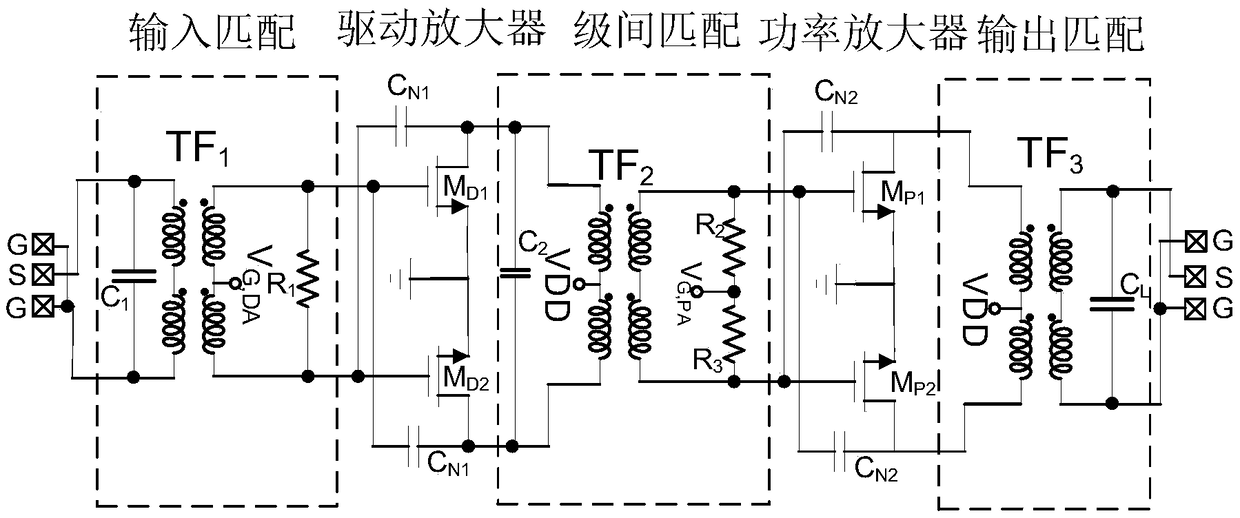
[0029] Such as figure 1 Shown is the broadband high gain flatness power amplifier of the present invention.

[0030] The single-ended signal entering the power amplifier first enters the input matching network and converts it into a differential double-ended signal. The amplitudes of the two signals are equal, and the phase difference is 180 degrees. The loss is smaller than that on both sides, thereby compensating for the large in-band fluctuation of the interstage matching, Figure 4 (a) is the input matching loss.

[0031] Then the two differential signals are sent to the drive amplifier and are amplified by the common source amplifier tube M D1 and M D2 Amplified, so that its output power can drive the back-end power amplifier after passing through the loss of the inter-stage matching network, and at the same time increase the gain of the total broadband power amplifier.

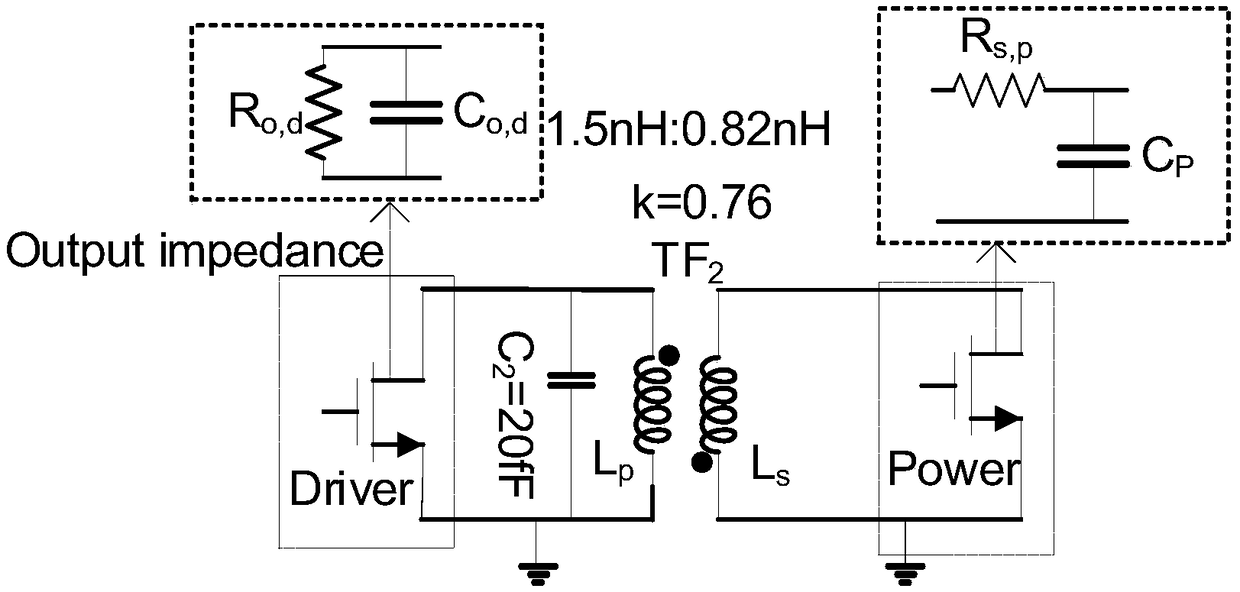
[0032] Afterwards, the two differential signals amplified by the drive amplifier are transmitted ...


PUM


Abstract

The invention belongs to the field of radio frequency microwave integrated circuit design, in particular to a broadband high-gain-flatness power amplifier. The power amplifier mainly includes: an input matching network composed of a high coupling factor transformer and a capacitor resistor; a differential common-source driver amplifier with neutralization capacitance; an inter-stage matching network composed of high coupling factor transformers; a differential common-source power amplifier with neutralizing capacitance for power amplification; and an output matching network which is composed of a high-coupling-factor transformer and a load capacitor. The power amplifier adopts high-coupling-factor transformers in three-stage matching network. The in-band gain fluctuation of broadband is reduced by compensating three-stage matched gain fluctuation, which effectively solves the problem of poor gain flatness caused by large inter-stage matched gain fluctuation of traditional broadband power amplifiers and improves the gain at the same time. Compared with the prior art, the invention can significantly improve the gain flatness of the wideband power amplifier while realizing high gain.

Description

technical field [0001] The invention belongs to the technical field of radio-frequency microwave integrated circuits, and in particular relates to a wide-band high-gain flatness power amplifier applied to radio-frequency phased array multifunctional transceiver components, which can be used in phased array systems such as wireless communication and radar detection. Background technique [0002] In recent years, with the continuous improvement of CMOS technology, the use of CMOS technology to implement power amplifiers has attracted more and more researchers' attention because of its low cost and high integration. In systems such as high-speed data communication, phased array radar, and software radio, high requirements are placed on the bandwidth and in-band gain flatness of power amplifiers. However, due to the low power supply voltage of the CMOS process and the large variation of input and output impedance with frequency, it is full of challenges to achieve high gain flat...

Claims


Application Information

Patent Timeline
Patent Type & Authority Applications(China)
IPC IPC(8): H03F1/02H03F1/14H03F1/18H03F3/213H03F3/45
CPCH03F1/0205H03F1/14H03F1/18H03F3/213H03F3/45264H03F3/45475
Inventor 李巍龚杰
Owner FUDAN UNIV
Why Eureka
Try Eureka