Nanowire transistor and forming method thereof

A transistor and nanowire technology, applied in the field of nanowire transistors and their formation, can solve the problems of large parasitic capacitance and poor performance of nanowire transistors, and achieve the effect of reducing parasitic capacitance and improving performance

Inactive Publication Date: 2019-01-15
SEMICONDUCTOR MANUFACTURING INTERNATIONAL (BEIJING) CORP +1
View PDF5 Cites 16 Cited by
  • Summary
  • Abstract
  • Description
  • Claims
  • Application Information

AI Technical Summary

Problems solved by technology

[0004] However, the distance between the gate and the source-drain doped layer of the nanowire transistor formed in the prior art is small, resulting in a large parasitic capacitance between the gate and the source-drain doped layer, which makes the performance of the nanowire transistor relatively low. Difference

Method used


Image

  • Nanowire transistor and forming method thereof
  • Nanowire transistor and forming method thereof
  • Nanowire transistor and forming method thereof

Examples


Embodiment Construction

[0034] There are many problems in the nanowire transistor in the prior art, for example, the parasitic capacitance between the gate and the source-drain doped layer is large, and the performance of the nanowire transistor is poor.

[0035] In combination with a method for forming a nanowire transistor, the reason why the performance of the nanowire transistor is poor due to the large parasitic capacitance between the gate and the source-drain doped layer of the nanowire transistor formed in the prior art is analyzed:

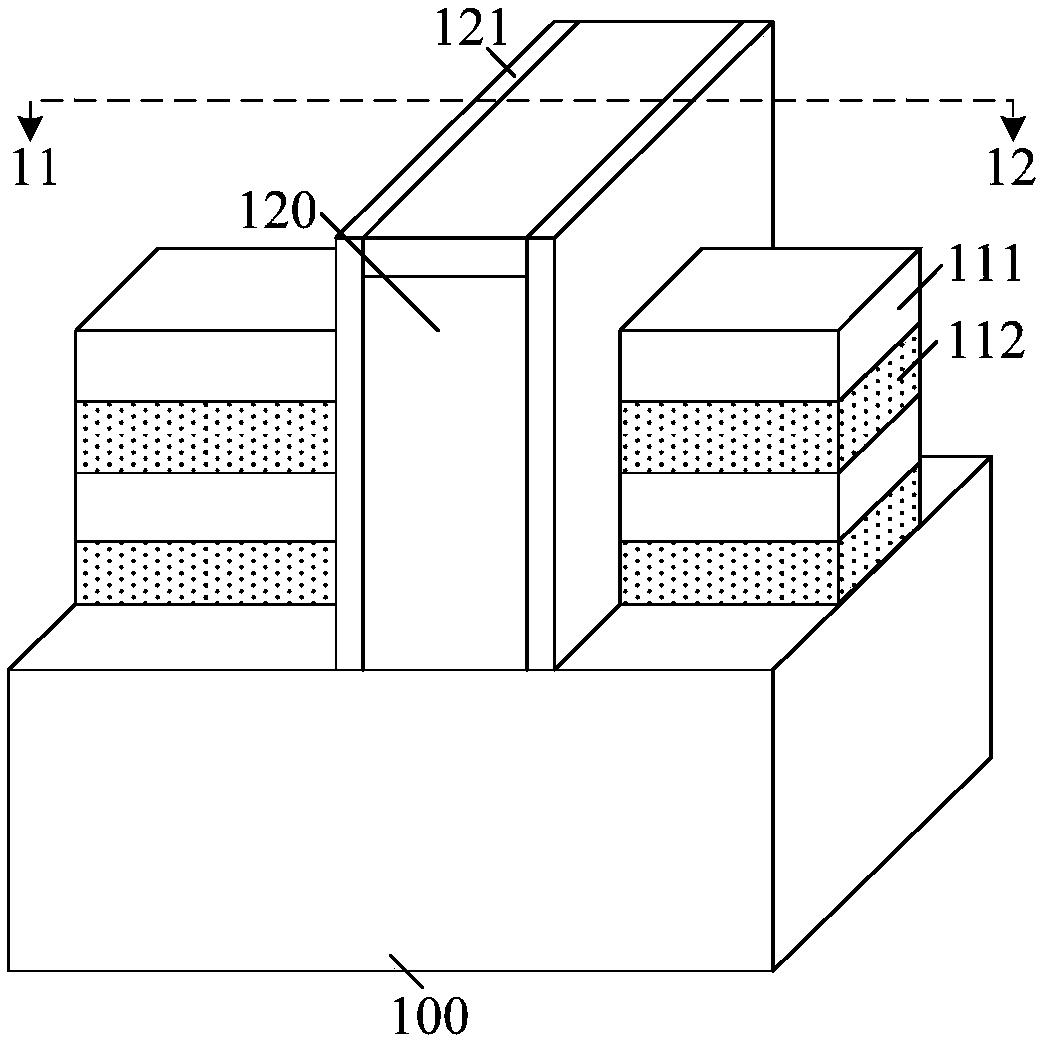
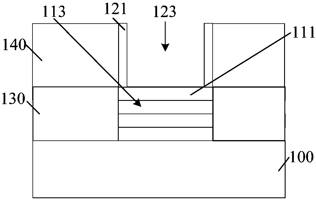
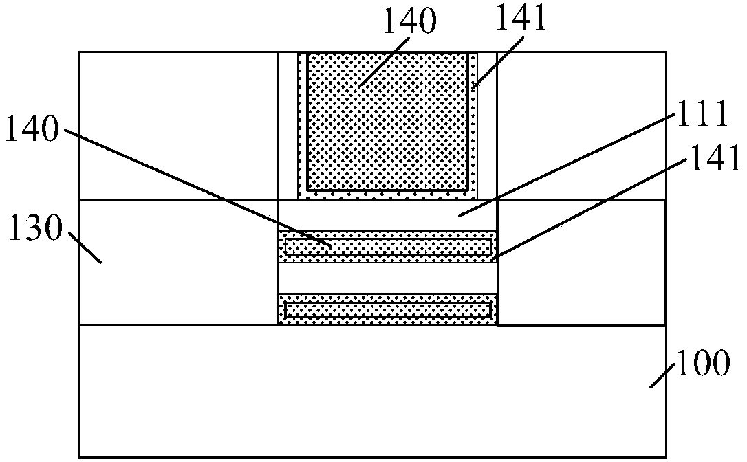
[0036] Figure 1 to Figure 3 It is a structural schematic diagram of each step of a method for forming a nanowire transistor.

[0037] Please refer to figure 1 , providing a substrate 100; forming a combined structure on the substrate 100, the combined structure includes a plurality of stacked combined layers, the combined layer includes a sacrificial layer 112 on the substrate 100 and a sacrificial layer located on the channel layer 111 on the sacrificial lay...


PUM

PropertyMeasurementUnit
widthaaaaaaaaaa
depthaaaaaaaaaa
thicknessaaaaaaaaaa

Abstract

The invention provides a nanowire transistor and a forming method thereof, wherein the forming method comprises the following steps of: providing a substrate; Forming a composite structure on the substrate, the composite structure comprising one or more laminated composite layers, the composite layers comprising a sacrificial layer on the substrate and a channel layer on the sacrificial layer, thechannel layer and the sacrificial layer being different in material; Etching a sacrificial layer of the side wall of the composite structure to form a depression on the surface of the side wall of the composite structure; Forming an isolation layer on the surface of the sacrificial layer exposed by the recess; Forming a source-drain doping layer on a substrate on both sides of the composite structure after forming the isolation layer, wherein the isolation layer is provided between the source-drain doping layer and the sacrificial layer; Removing the remaining sacrificial layer after the source-drain doping layer is formed; Forming a gate structure surrounding the channel layer. The resulting transistor reduces parasitic capacitance and improves transistor performance.

Description

technical field [0001] The invention relates to the technical field of semiconductor manufacturing, in particular to a nanowire transistor and a forming method thereof. Background technique [0002] With the development of semiconductor technology, the feature size of semiconductor devices is not much reduced. After the device size enters the deep submicron size, the short channel effect becomes an obstacle to the continuous miniaturization of traditional planar transistors. This stems from a decrease in gate control capability coupled with an increasing influence of the drain on the bulk potential. [0003] Nanowire transistors (NWFETs) promise to solve this problem. On the one hand, the small channel thickness and width make the gate of the nanowire transistor closer to each part of the channel, which helps to enhance the gate capability of the transistor, and most of the nanowire transistors adopt a gate-enclosed structure, and the gate is viewed from all directions. M...

Claims


Application Information

Patent Timeline
Patent Type & Authority Applications(China)
IPC IPC(8): H01L29/78H01L29/06H01L21/336
CPCB82Y10/00H01L29/0653H01L29/66545H01L29/66553H01L29/78
Inventor 唐粕人
Owner SEMICONDUCTOR MANUFACTURING INTERNATIONAL (BEIJING) CORP
Why Eureka
Try Eureka