
Silicon photonic optical transceiver module

An optical transceiver module and silicon photonics technology, applied in the field of optical communication, can solve the problems of radio frequency crosstalk, affect the performance of optical modules, increase the difficulty of miniaturization and packaging of optical modules, etc., and achieve low high-frequency transmission loss and short electrical signal connection paths. , Improve the effect of high frequency suppression problem

Inactive Publication Date: 2019-01-18
GUANGXUN SCI & TECH WUHAN
View PDF8 Cites 19 Cited by
  • Summary
  • Abstract
  • Description
  • Claims
  • Application Information

AI Technical Summary

Problems solved by technology

However, at present, the optical module generally adopts the method of gold wire bonding, which often brings radio frequency crosstalk and affects the performance of the optical module.
On the other hand, more and more functions are integrated in the optical module, and more and more devices are included in the optical module, which increases the difficulty of miniaturization and packaging of the optical module.

Method used


Image

  • Silicon photonic optical transceiver module
  • Silicon photonic optical transceiver module
  • Silicon photonic optical transceiver module

Examples


Embodiment 1

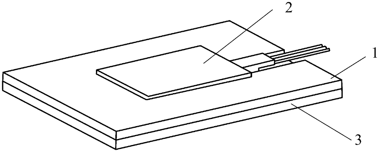
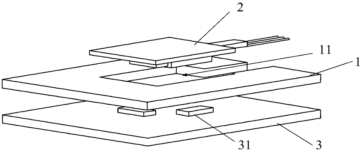
[0033] Please also refer to Figure 1 to Figure 4 This embodiment provides a silicon-optical optical transceiver module, the silicon-optical optical transceiver module includes a circuit board 1 and an optical component 2 , the circuit board 1 is provided with a hollow area 11 , and the hollow area 11 is used for accommodating the optical component 2 . The circuit board 1 is provided with a plurality of first pads 12 along the periphery of the hollow area 11 , and a plurality of second pads 22 are provided on the edge of the optical component 2 . The pads 12 and the corresponding second pads 22 are attached to each other to realize electrical connection.

[0034] The cross-sectional shape and size of the hollow area 11 are determined according to the cross-sectional shape and size of the optical component 2. The cross-sectional shape of the hollow area 11 is basically the same as the cross-sectional shape of the optical component 2, and it is necessary to ensure that the optic...


PUM


Abstract

The invention discloses a silicon photonic optical transceiver module. The silicon photonic optical transceiver module comprises a circuit board and an optical component; the circuit board is arrangedin a hollow region, and the hollow region is used for accommodating the optical component; the circuit board is provided with a plurality of first bonding pads along the periphery of the hollow region; a plurality of second bonding pads are arranged at the edge of the optical component; and after the optical component and the circuit board are attached in a reverse mounting mode, the second bonding pads are attached to the corresponding first bonding pads so as to implement electrical connection. The electrical connection is established between the circuit board and the optical component by the first bonding pads and the second bonding pads, an electric signal connection path is short, a stray capacitance is small, high-frequency transmission loss is low, high-frequency characteristics are improved, and the problem of high-frequency inhibition caused by a gold-wire bonding wire currently can be effectively improved. Meanwhile, the optical component and the circuit board are attached in a reverse buckling mode, the design structure is compact, and the size of the silicon photonic optical transceiver module can be effectively reduced.

Description

technical field [0001] The invention belongs to the field of optical communication, and more particularly, relates to a silicon-optical optical transceiver module. Background technique [0002] At present, silicon photonics technology is becoming more and more mature, and its advantages such as high integration, small size, low power consumption, and optoelectronic integration have attracted much attention. In the future, silicon photonics technology will likely replace the current free space coupling technology, and silicon photonics technology has long-term solutions. The ability of technological evolution (high speed, high integration) and cost conflict. [0003] With the continuous improvement of the transmission rate of optical modules, from 32Gbps to 64Gbps, the data communication module has achieved 100Gb / s transmission at a single wavelength, and the backbone network and metropolitan area network coherent optical modules have achieved single wavelength 400Gb / s transm...

Claims


Application Information

Patent Timeline
Patent Type & Authority Applications(China)
IPC IPC(8): G02B6/42
CPCG02B6/4239G02B6/424G02B6/4245G02B6/428
Inventor 梁雪瑞马卫东张博胡毅
Owner GUANGXUN SCI & TECH WUHAN
Learn More