Image sensor and forming method thereof

An image sensor and ion implantation technology, which is used in the manufacture of electrical solid-state devices, semiconductor devices, and semiconductor/solid-state devices. The ability to store photoelectrons, the effect of increasing the full well capacity

Inactive Publication Date: 2019-01-18
HUAIAN IMAGING DEVICE MFGR CORP
View PDF3 Cites 4 Cited by
  • Summary
  • Abstract
  • Description
  • Claims
  • Application Information

AI Technical Summary

Problems solved by technology

[0003] However, with the development of technology and the expansion of the market, the size of CMOS image sensors is gradually reduced, and the area of ​​photodiodes is also reduced accordingly. The most direct impact is the reduction of the full well capacity of the sensor.

Method used


Image

  • Image sensor and forming method thereof
  • Image sensor and forming method thereof
  • Image sensor and forming method thereof

Examples


Embodiment 1

[0031] Figure 2-Figure 7 Provided is a method for forming a partial device layer structure of a back-illuminated CMOS image sensor.

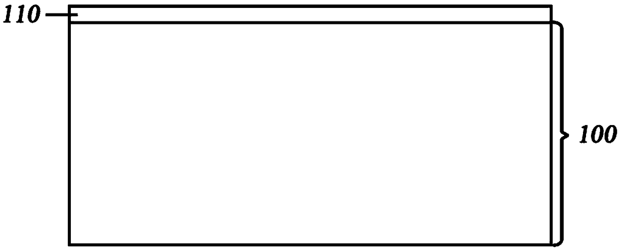
[0032] refer to figure 2 , providing a semiconductor substrate 100 and forming a protection layer 110 covering the semiconductor substrate 100 .

[0033] In a specific implementation, the semiconductor substrate 100 may be a silicon substrate, or the material of the semiconductor substrate 100 may also be germanium, silicon germanium, silicon carbide, gallium arsenide, or gallium indium. The bottom 100 may also be a silicon substrate on an insulator surface or a germanium substrate on an insulator surface, or a substrate grown with an epitaxial layer (Epitaxy layer, Epi layer).

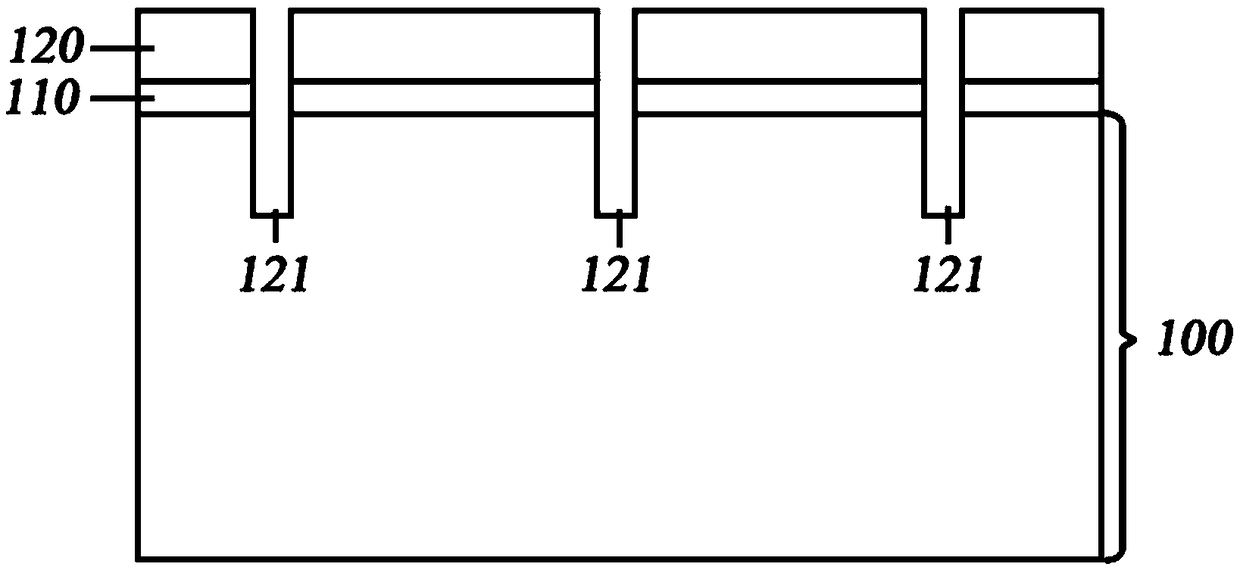
[0034] Preferably, the semiconductor substrate 100 is a lightly doped semiconductor substrate, and the doping type is opposite to that of the photodiodes formed in the semiconductor substrate 100 in subsequent processes. Specifically, deep well implantation (Deep W...

Embodiment 2

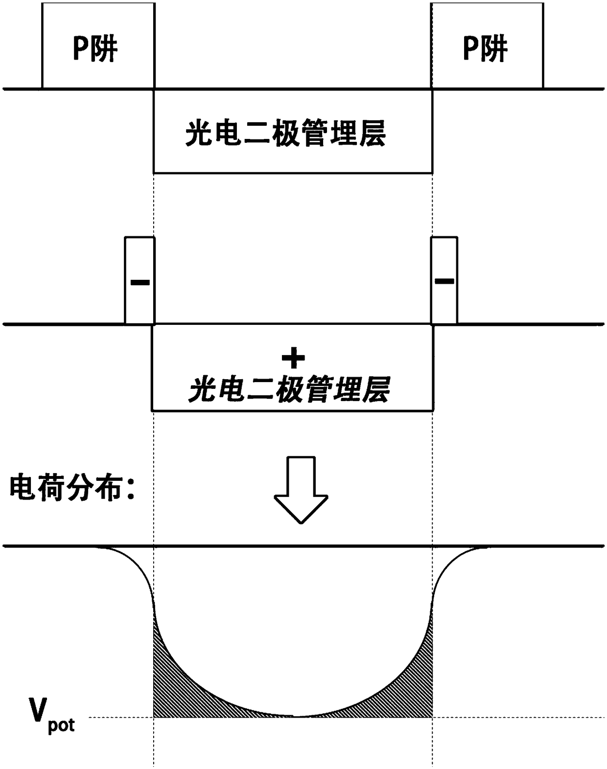
[0060] This embodiment is relatively close to Embodiment 1, but slightly different. The difference is that in this embodiment, after the buried layer 132 of the photodiode is formed through the first doping, the buried layer 132 is doped by using different ion implantation processes.

[0061] refer to Figure 9 , remove the second mask layer 130, re-form a third mask layer 140 on the protective layer 110, pattern the third mask layer 140, and expose the edge region 142 of the buried layer 132; In the third ion implantation process, a third doping is performed on the edge region 142 of the buried layer 132 .

[0062] The third doping uses the same type of doping ions as the first doping. In this embodiment, the doping ions used in the first ion implantation process are N-type ions As, and the third ions The dopant ions used in the implantation process are also As, and the energy is about 50-300 KeV higher than the ion energy used in the first ion implantation process. In thi...


PUM


Abstract

The invention provides a method for forming an image sensor, comprising the following steps: providing a photodiode region; performing a first doping on the photodiode region by a first ion implantation process to form a buried layer; performing a second doping opposite to the first doping on a central region of the buried layer by a second ion implantation process, or performing the third dopinghaving the same type as the first doping on an edge region of the buried layer by a third ion implantation process. The technical proposal provided by the invention can effectively improve the gradient of the electric potential change in the buried layer edge region, so that the electric potential in the region rapidly changes from low to high, thereby improving the photodiode storage capacity ofphotoelectrons and effectively improving the full well capacity. In addition, using the opposite type of second doping can also effectively prevent the occurrence of image smearing in the center region.

Description

technical field [0001] The invention relates to the field of semiconductor design and manufacture, and more specifically, the invention relates to an image sensor and a forming method thereof. Background technique [0002] Full well capacity (Full Well Capacity, FWC) is an important parameter to characterize the performance of photodiodes, which refers to the maximum number of electrons that can be carried in the capacitance of photodiodes. Larger full well capacity can make the CMOS image sensor (CMOS Image Sensor, CIS) unit have higher dynamic range, higher signal-to-noise ratio and sensitivity. It can be said that the size of the full well capacity can fundamentally determine the overall performance of pixel imaging. [0003] However, with the development of technology and the expansion of the market, the size of the CMOS image sensor is gradually reduced, and the area of ​​the photodiode is also reduced accordingly. The most direct impact is the reduction of the full we...

Claims


Application Information

Patent Timeline
Patent Type & Authority Applications(China)
IPC IPC(8): H01L27/146H01L21/265
CPCH01L21/26513H01L27/1463H01L27/1464H01L27/14683
Inventor 刘斌武吕相南北村阳介
Owner HUAIAN IMAGING DEVICE MFGR CORP
Why Eureka
Try Eureka