A manufacturing method of a white light LED chip
A technology of LED chips and manufacturing methods, which is applied in the direction of electrical components, circuits, semiconductor devices, etc., can solve the problems of white LEDs such as high power density, poor color reproduction, and discontinuous wavelength, so as to ensure light output efficiency and uniformity of light output , Low production cost, continuous wavelength effect
- Summary
- Abstract
- Description
- Claims
- Application Information
AI Technical Summary
Problems solved by technology
Method used
Image
Examples
Embodiment 1
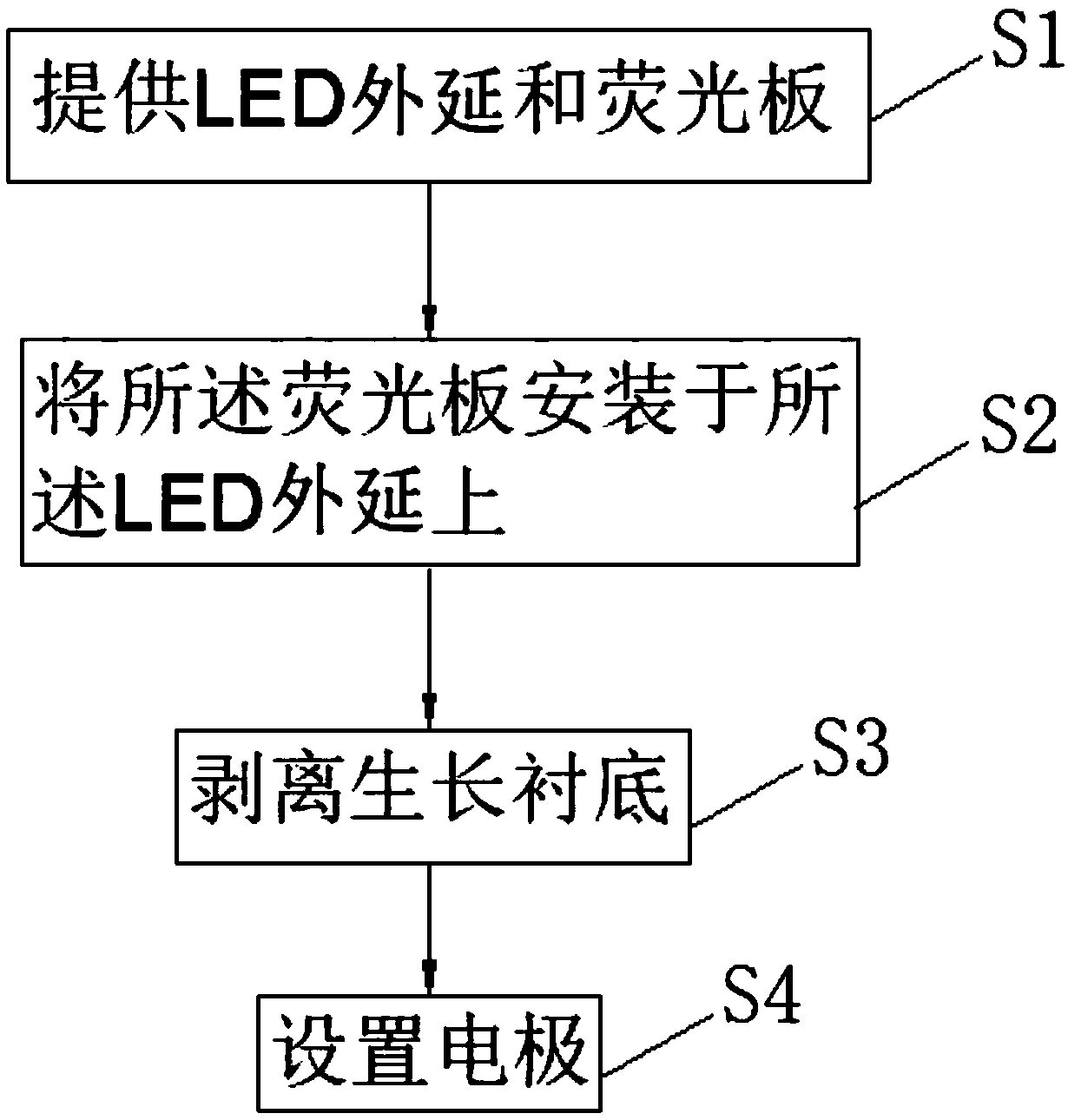
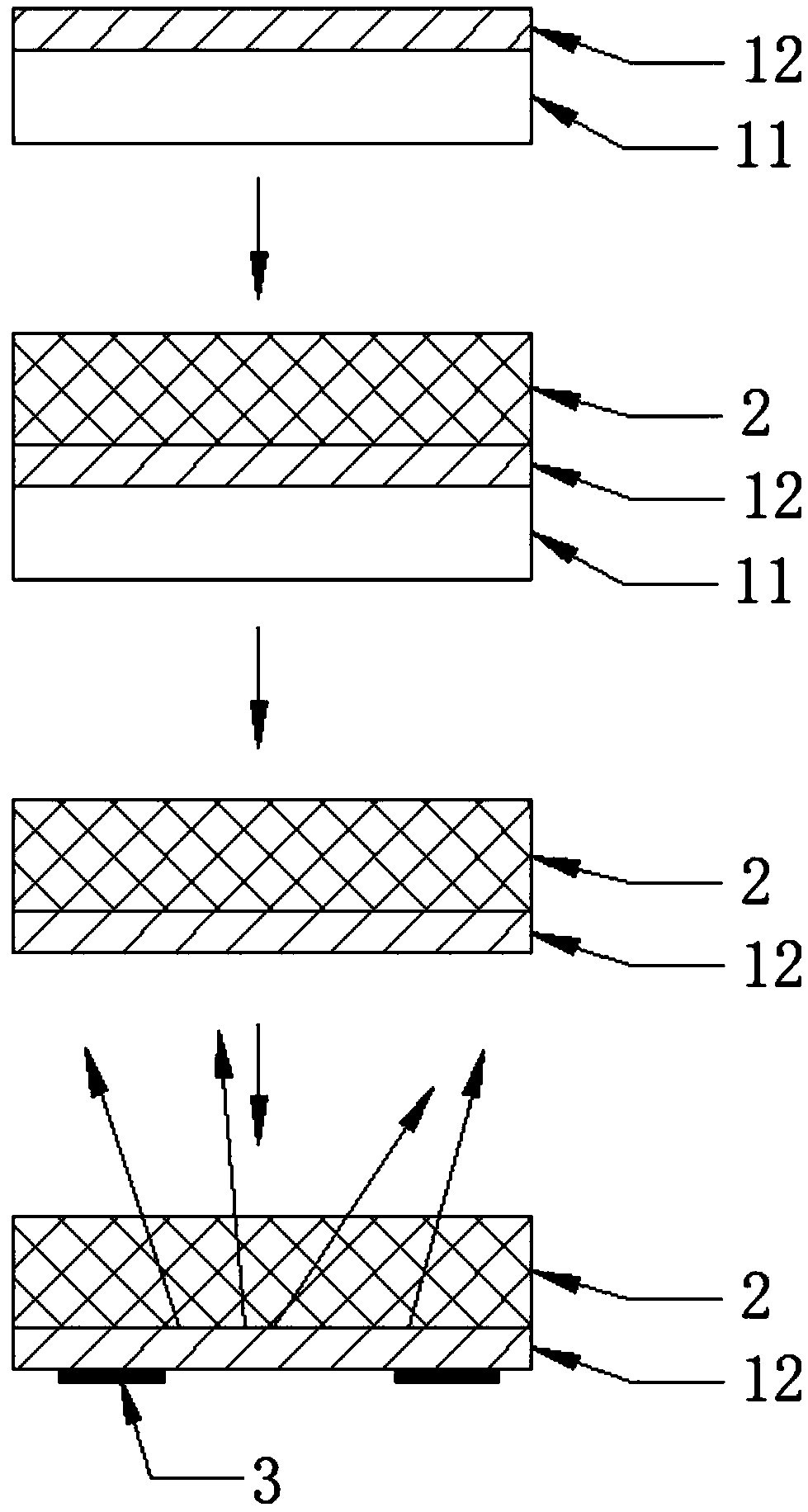
[0054] Such as Figure 1-2 Shown, a kind of manufacturing method of white light LED chip comprises the following steps:
[0055] S1. Provide an LED epitaxy 1 and a phosphor plate 2, the LED epitaxy 1 includes a growth substrate 11 and a light-emitting layer 12 grown on the growth substrate 11, wherein the light-emitting layer 12 includes N-GaN layers 121 arranged in sequence , a quantum well layer 122 and a P-GaN layer 123, wherein the N-GaN layer 121 is connected to the growth substrate 11.
[0056] The growth substrate 11 is one of a sapphire substrate, a silicon carbide substrate, a silicon substrate or a gallium nitride substrate, and the growth substrate is selected according to actual needs.
[0057]Wherein, the fluorescent plate 2 is formed by mixing fluorescent powder and a transparent high-temperature-resistant material. Specifically, the transparent high-temperature-resistant material is sapphire, glass, quartz crystal or silicon carbide. The phosphor is one or mor...
Embodiment 2
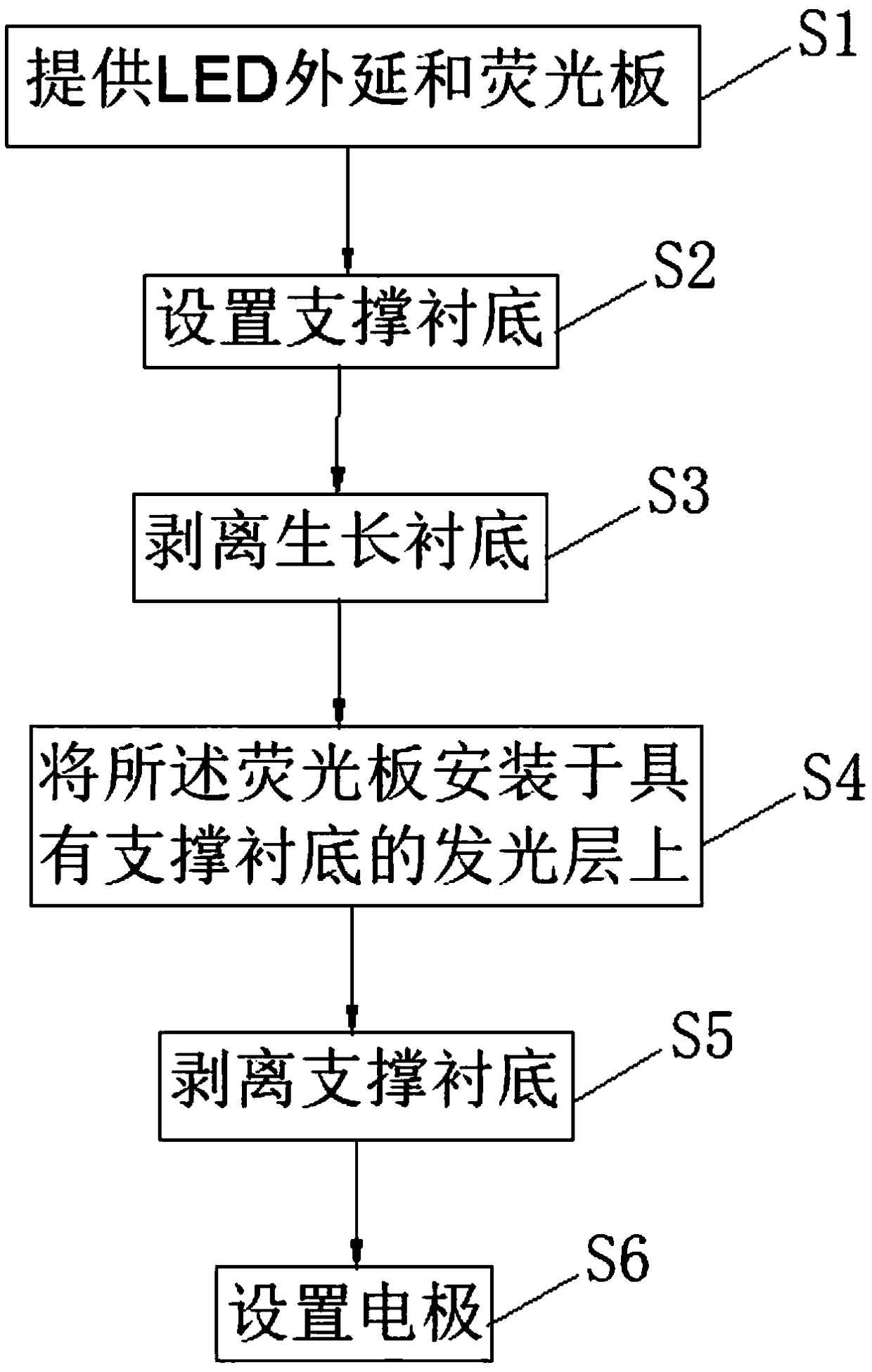
[0065] Such as Figure 3-5 As shown, this embodiment, as an improved implementation of the first embodiment, solves the problem that the luminous efficiency and the light uniformity of the white LED chip cannot be maximized.
[0066] A method for manufacturing a white light LED chip, comprising the following steps:
[0067] S1. Provide an LED epitaxy 1 and a phosphor plate 2, the LED epitaxy 1 includes a growth substrate 11 and a light-emitting layer 12 grown on the growth substrate 11, wherein the light-emitting layer 12 includes N-GaN layers 121 arranged in sequence , a quantum well layer 122 and a P-GaN layer 123, wherein the N-GaN layer 121 is connected to the growth substrate 11.
[0068] The growth substrate 11 is one of a sapphire substrate, a silicon carbide substrate, a silicon substrate or a gallium nitride substrate, and the growth substrate is selected according to actual needs.
[0069] Wherein, the fluorescent plate 2 is formed by mixing fluorescent powder and ...
Embodiment 3
[0078] Such as Figure 6-7 As shown, this embodiment serves as an improved implementation of the above-mentioned embodiment, and solves the problem of low production efficiency of white light LED chips.
[0079] A method for manufacturing a white light LED chip, comprising the following steps:
[0080] S1. Provide an LED wafer 5 and a phosphor plate 2, the LED wafer 5 includes a growth substrate 51, a light emitting layer 52, an ohmic contact layer 53, an insulating layer 53, and an electrode layer 55 arranged in sequence, wherein the light emitting layer The number of 52 is at least one, which includes an N-GaN layer, a quantum well layer and a P-GaN layer arranged in sequence, wherein the N-GaN layer is connected to the growth substrate.
[0081] The growth substrate 51 is one of a sapphire substrate, a silicon carbide substrate, a silicon substrate or a gallium nitride substrate, and the growth substrate is selected according to actual needs.
[0082] Wherein, the fluores...
PUM
 Abstract
Description
Claims
Application Information


