Method for enhancing single-layer graphene broadband absorption based on strong coupling effect
A single-layer graphene and strong coupling technology, applied in the field of nanophotonics, can solve the problems of low device performance, absorption fluctuations, limitations, etc., and achieve the effects of small intrinsic loss, high ultrafast modulation, and high modulation bandwidth
- Summary
- Abstract
- Description
- Claims
- Application Information
AI Technical Summary
Problems solved by technology
Method used
Image
Examples
Embodiment 1
[0031] Embodiment 1: as figure 1 As shown, a design structure based on the strong coupling effect to enhance the broadband absorption of single-layer graphene, including the graphene nanoribbon array of the absorbing layer and the metal trapezoidal groove substrate structure.
[0032] Among them, the graphene strip array period is 2 μm, the strip width is 67 nm, and the substrate trapezoidal metal groove structure has a top width of 300 nm, a bottom width of 700 nm, and a groove height of 1.4 μm. The metal material of the substrate layer is selected from silver, a metal with low intrinsic loss.
[0033] In this example, the graphene nanoribbons of the absorbing layer are only in contact with one side of the metal trapezoidal groove, thereby ensuring that the excited graphene surface plasmon resonance has less intrinsic loss, thereby promoting the system Excitation of strong coupling effects.
Embodiment 2
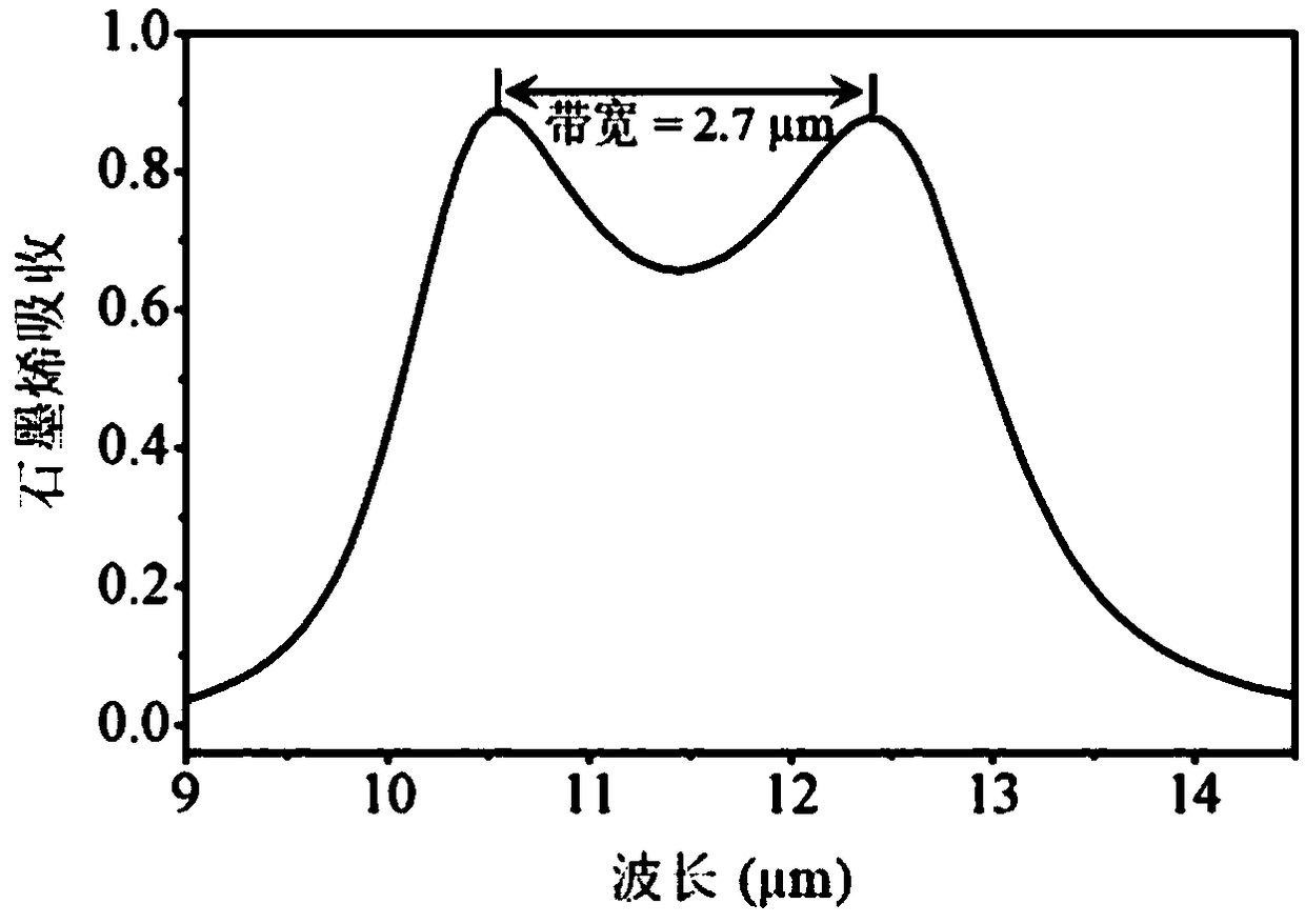
[0034] Embodiment 2: as figure 2 and 3 as shown, figure 2 The broadband graphene absorption spectrum generated for this design, when the transverse magnetic (TM) wave is perpendicular to the sample surface, the structure can simultaneously excite the graphene surface plasmon resonance and magnetic resonance. Due to the extremely narrow top trough width limitation, the hybrid mode field caused by the strong coupling between the two modes will be mainly bound at the graphene, resulting in a broadband graphene absorption effect.
[0035] From figure 2 It can be seen that the use of this structure can produce a huge broadband graphene absorption effect with a bandwidth of 2.7 μm, and the absorption rate is 60%, far exceeding the absorption efficiency of single-layer graphene which is only 2.3%.
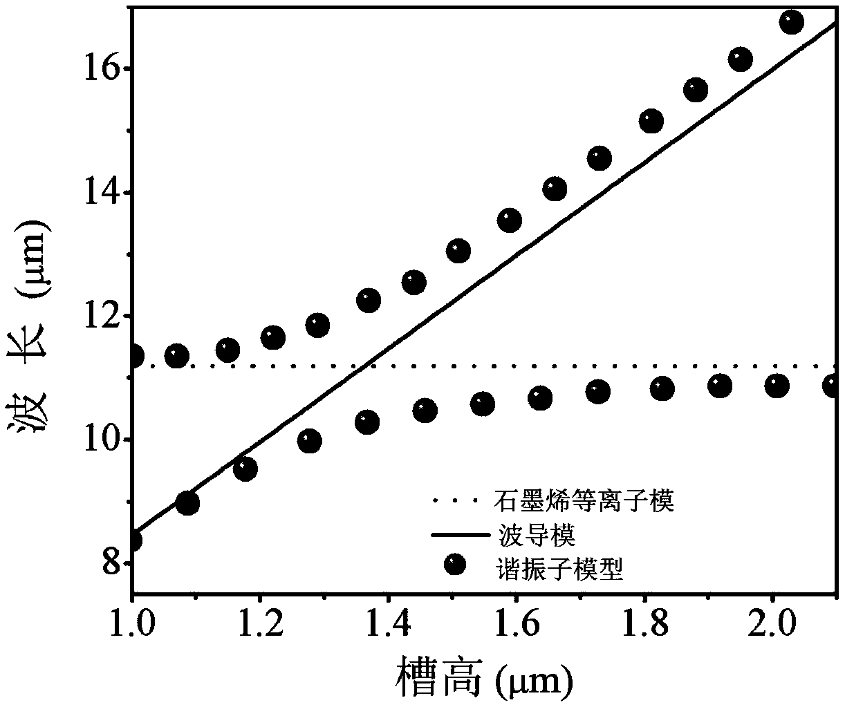
[0036] image 3 The dispersion curves of the magnetic resonance mode and the graphene plasmon mode are given, which can clearly prove that the broadband absorption effect caused by...
Embodiment 3
[0037] Embodiment 3: as Figure 4 As shown, the specific preparation flow chart of the selected graphene broadband absorption structure based on strong coupling effect enhancement;
[0038] 1) Coating: Coating a layer of 1.4 micron-thick filling dielectric film on the metal substrate, wherein the metal substrate is silver, and the dielectric material of the coating is silicon dioxide;
[0039] 2) Etching: UV etching is performed on the filling medium, and a trapezoidal dielectric array structure is constructed by etching;
[0040] 3) Sputtering metal: sputtering metal on the etched sample, the material is silver which is the same as the metal of the substrate;
[0041] 4) Post-processing: After engraving or polishing, remove the excess metal material on the surface of the sample after magnetron sputtering;
[0042] 5) transfer: graphene is transferred to the upper surface of the post-treated sample;
[0043] 6) Forming: After transferring the processed sample, a graphene na...
PUM
 Abstract
Description
Claims
Application Information


