mram array and its manufacturing method

A manufacturing method and array technology, applied in the manufacture/processing of electromagnetic devices, semiconductor devices, electrical components, etc., can solve problems such as poor chip uniformity, achieve good uniformity, and shorten removal time

Active Publication Date: 2021-01-22
CETHIK GRP +1
View PDF5 Cites 0 Cited by
  • Summary
  • Abstract
  • Description
  • Claims
  • Application Information

AI Technical Summary

Problems solved by technology

[0008] The main purpose of this application is to provide an MRAM array and its manufacturing method to solve the problem of poor chip uniformity caused by the inability to quickly remove low-K dielectric materials in the prior art

Method used


Image

  • mram array and its manufacturing method
  • mram array and its manufacturing method
  • mram array and its manufacturing method

Examples


Embodiment 1

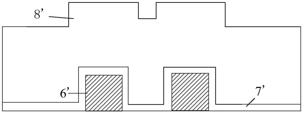
[0082] A substrate 1 including a base and structures prepared through previous processes on the base is prepared.

[0083] On the substrate 1, a copper metal layer is deposited by a damascene process (the isolation dielectric layer 11 is arranged on the substrate, and then holes are opened in the isolation dielectric layer, and metal copper is filled in the holes), forming a plurality of connection metal layers 2, and more The surface of the connection metal layer 2 away from the substrate is on the same plane, such as Figure 10 shown.

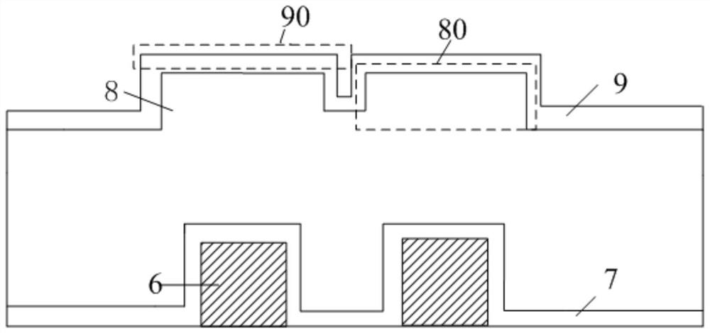
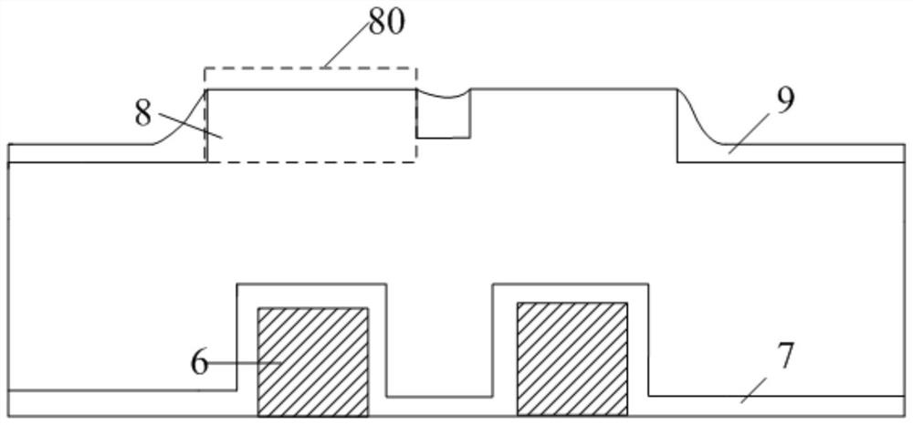
[0084] N-BLOK is deposited on the surface of each connecting metal layer 2 away from the substrate 1 to form a barrier layer 3 . Formation of SiO by PECVD on barrier layer 3 using TEOS 2 layer, that is, the first isolation layer 41 .

[0085] First through holes are opened in the barrier layer 3 and the first isolation layer 41 on each of the connecting metal layers 2 , and the first through holes correspond to the connecting metal layers ...

Embodiment 2

[0097] The difference from Example 1 is that the thickness of the MTJ unit is the same as that of the low-K dielectric layer, both And after removing the first raised portion and the remaining polishing barrier layer, it is only necessary to use chemical mechanical polishing to remove the protective layer 7 on the plane where the first surface is located, and then deposit Ta on the first surface and the above-mentioned dielectric unit, and engrave The excess Ta is etched to form the top electrode.


PUM


Abstract

The present application provides an MRAM array and a manufacturing method thereof. The manufacturing method includes: step S1, setting a pre-storage structure including MTJ units on the surface of the substrate, the surface of the MTJ unit away from the substrate being the first surface; step S2, setting a dielectric unit on the MTJ unit, the dielectric unit comprising The low-K dielectric layer and the polishing barrier layer, the thickness of the low-K dielectric layer is greater than or equal to the thickness of the MTJ unit, the thickness of the polishing barrier layer is less than the thickness of the low-K dielectric layer, and the low-K dielectric layer and the polishing barrier layer respectively include The first raised portion and the second raised portion; Step S3, removing the second raised portion; Step S4, removing at least the first raised portion and the remaining polishing barrier layer, so that the surface of the remaining media unit is a continuous plane, Or make the surface of the remaining low-K dielectric layer on both sides of the MTJ unit be on the same plane as the first surface. This method makes the MTJ unit have better uniformity.

Description

technical field [0001] The present application relates to the field of semiconductor technology, in particular, to an MRAM array and a manufacturing method thereof. Background technique [0002] Magnetic Random Access Memory (MRAM) is a new type of non-volatile memory. Compared with other types of memory at present, it has fast read and write speeds, can achieve unlimited erasing and writing, and is easy to integrate with current semiconductor processes. In addition, the spin transfer torque (Spin transfer torque, STT) MRAM array using spin current to achieve magnetic moment reversal can realize the miniaturization of the memory cell size. These advantages make MRAM the main development direction of new memory in the future. [0003] The main functional unit in MRAM is MTJ unit, and its structure mainly includes magnetic free layer / nonmagnetic oxide layer (MgO) / magnetic pinning layer. Driven by an external magnetic field or current, the direction of the magnetic moment of ...

Claims


Application Information

Patent Timeline
Patent Type & Authority Patents(China)
IPC IPC(8): H01L27/22H01L43/12
CPCH10B61/00H10N50/01
Inventor 王雷刘鲁萍
Owner CETHIK GRP
Why Eureka
Try Eureka