Semiconductor device and manufacturing method thereof

A manufacturing method and semiconductor technology, applied in the direction of semiconductor/solid-state device manufacturing, semiconductor devices, semiconductor/solid-state device components, etc., can solve problems such as bump voids, prevent voids, improve roughness, and increase polishing time. Effect

Active Publication Date: 2020-11-06
淮安西德工业设计有限公司
View PDF7 Cites 0 Cited by
  • Summary
  • Abstract
  • Description
  • Claims
  • Application Information

AI Technical Summary

Problems solved by technology

However, in the process of chemical mechanical polishing, there is a certain pressure between the polishing pad and the bump. When the bump is polished to be flush with the surface of the substrate, the center of the bump will be lower than the periphery. During the bonding process, resulting in voids between the bonded bumps

Method used


Image

  • Semiconductor device and manufacturing method thereof
  • Semiconductor device and manufacturing method thereof
  • Semiconductor device and manufacturing method thereof

Examples


no. 1 example

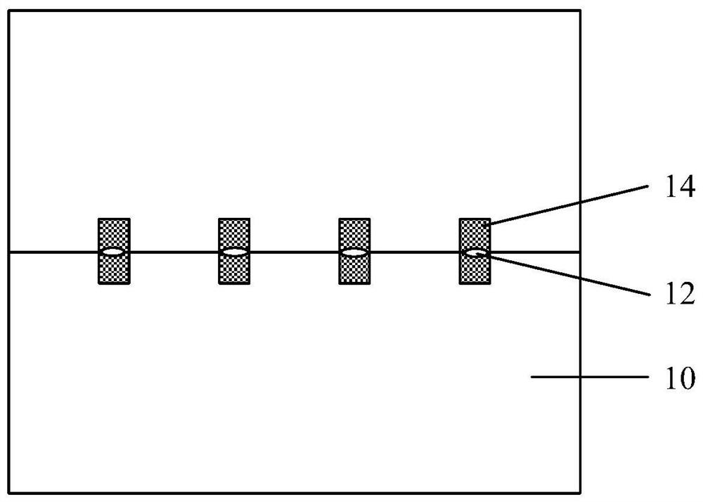
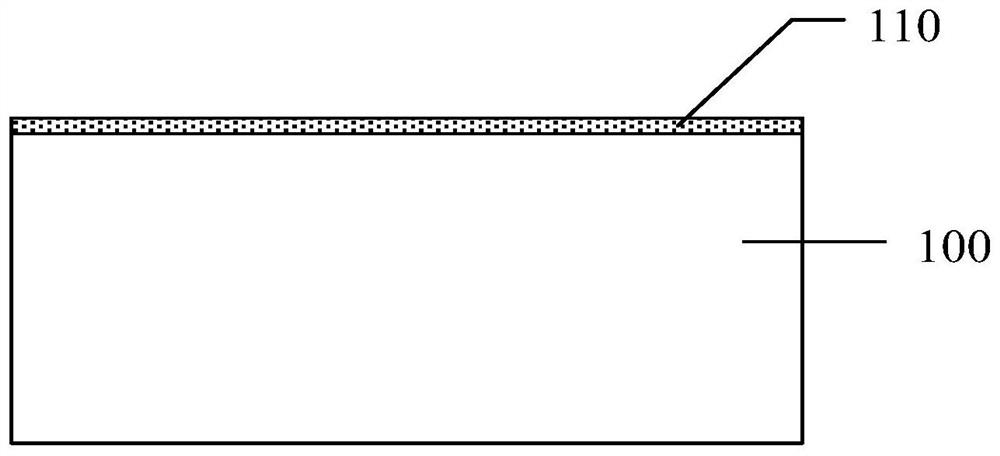
[0030] Figure 2 to Figure 6 It is a structural diagram corresponding to each step of forming a semiconductor device according to the first embodiment of the present invention. refer to figure 2 , providing a substrate 100 on which a metal oxide layer 110 is formed.

[0031] In this embodiment, the method for forming the metal oxide layer 110 may be chemical vapor deposition. The material of the metal oxide layer may be zinc oxide or aluminum oxide.

[0032] In this embodiment, the base 100 may be a semiconductor substrate, or a semiconductor substrate on which other semiconductor elements have been formed.

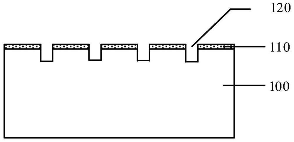
[0033] refer to image 3 , etching the metal oxide layer 110 and the substrate 100 to form a trench 120 .

[0034] In this embodiment, the method for etching the metal oxide layer 110 and the substrate 100 may be a dry etching process, and the gas used is C 4 f 8 or CF 4 .

[0035] refer to Figure 4 , forming a metal layer 130 on the metal oxide layer 110 , an...

no. 2 example

[0045] Compared with the first embodiment, the second embodiment differs in that after forming the metal oxide layer 110 and before forming the trench 120 , it further includes: forming an insulating layer 140 on the metal oxide layer 110 .

[0046] Figure 7 to Figure 11 It is a schematic structural diagram corresponding to each step of forming a semiconductor device according to the second embodiment of the present invention. refer to Figure 7 , providing a substrate 100 , forming a metal oxide layer 110 on the substrate 100 ; and forming an insulating layer 140 on the metal oxide layer 110 .

[0047] In this embodiment, the method for forming the metal oxide layer 110 may be chemical vapor deposition. The material of the metal oxide layer may be zinc oxide or aluminum oxide.

[0048]In this embodiment, the method for forming the insulating layer 140 may be chemical vapor deposition, and the material of the insulating layer 140 may be silicon oxide or silicon oxynitride....


PUM


Abstract

The invention discloses a semiconductor device and a manufacturing method thereof. The manufacturing method comprises the steps of: providing a substrate; forming a metal oxide layer on the substrate;etching the metal oxide layer and a semiconductor substrate to form a groove; forming a metal layer on the metal oxide layer so as to fulfill the groove; removing the metal layer on the surface of the metal oxide layer; and removing the metal oxide layer to form metal lugs, wherein the heights of the edges of the metal lugs are higher than the surface of the substrate. Finally, the fusion combination among the metal lugs eliminates the gap problem caused by defects on the surfaces of the metal lugs, thereby improving the yield of the semiconductor after bonding.

Description

technical field [0001] The invention relates to the field of semiconductor manufacturing, in particular to a semiconductor device and a manufacturing method thereof. Background technique [0002] With the continuous advancement and development of CMOS technology, the number of transistors is increasing, resulting in smaller and smaller interconnect sizes, and the problem of signal delay is becoming more and more serious, which has become a key factor affecting the improvement of system speed. The use of 3D integrated chip stacking technology will help greatly reduce wiring length, shorten signal delay, reduce power consumption, and at the same time reduce chip size, thereby improving the system performance of the device. The emergence of new device structures will drive the development of new packaging processes. Therefore, many existing packaging methods will be replaced by new chip-level, high-density metal bump (such as copper pillar bump Cupillar) structural packaging. ...

Claims


Application Information

Patent Timeline
Patent Type & Authority Patents(China)
IPC IPC(8): H01L21/60H01L23/488
CPCH01L24/11H01L24/14H01L24/81H01L2224/11614H01L2224/1184H01L2224/141H01L2224/818H01L2224/81902
Inventor 马敬金子貴昭黄晓橹
Owner 淮安西德工业设计有限公司
Why Eureka
Try Eureka