Check patentability & draft patents in minutes with Patsnap Eureka AI!

A light-emitting diode epitaxial wafer and its preparation method

A technology of light-emitting diodes and epitaxial wafers, applied in semiconductor devices, electrical components, circuits, etc., can solve problems such as mismatch between electron and hole injection, and achieve the effects of improving injection efficiency, prolonging time, and slowing down migration rate

Active Publication Date: 2021-04-27
HC SEMITEK ZHEJIANG CO LTD
View PDF23 Cites 0 Cited by
  • Summary
  • Abstract
  • Description
  • Claims
  • Application Information

AI Technical Summary

Problems solved by technology

[0006] The embodiment of the present invention provides a light-emitting diode epitaxial wafer and its preparation method, which can solve the problem of mismatching injection of electrons and holes in the prior art

Method used


Image

  • A light-emitting diode epitaxial wafer and its preparation method
  • A light-emitting diode epitaxial wafer and its preparation method
  • A light-emitting diode epitaxial wafer and its preparation method

Examples


Embodiment Construction

[0029] In order to make the object, technical solution and advantages of the present invention clearer, the implementation manner of the present invention will be further described in detail below in conjunction with the accompanying drawings.

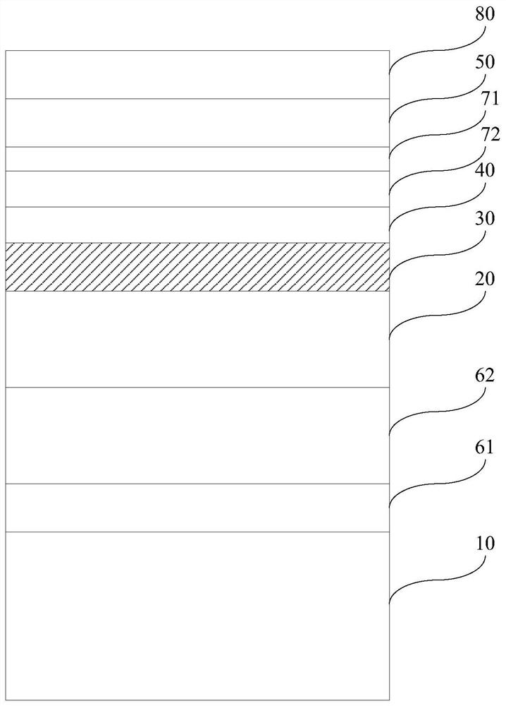
[0030] An embodiment of the present invention provides a light emitting diode epitaxial wafer. figure 1 A schematic structural diagram of a light emitting diode epitaxial wafer provided by an embodiment of the present invention. see figure 1 , the light-emitting diode epitaxial wafer includes a substrate 10, an N-type semiconductor layer 20, a carrier adjustment layer 30, an active layer 40 and a P-type semiconductor layer 50, an N-type semiconductor layer 20, a carrier adjustment layer 30, an active Layer 40 and P-type semiconductor layer 50 are sequentially stacked on substrate 10 .

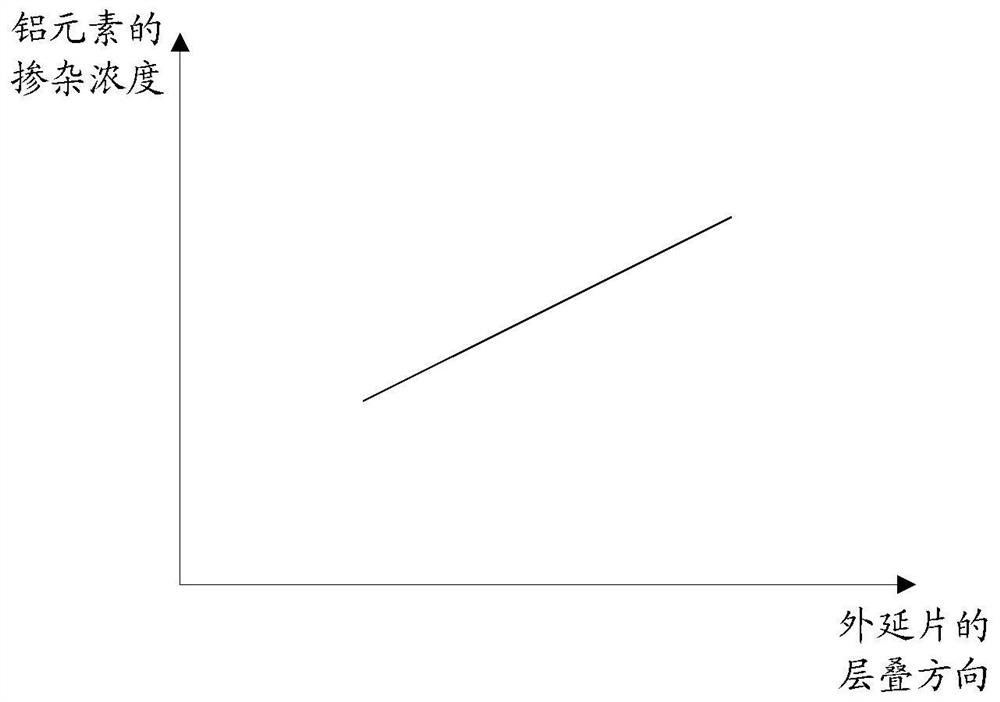
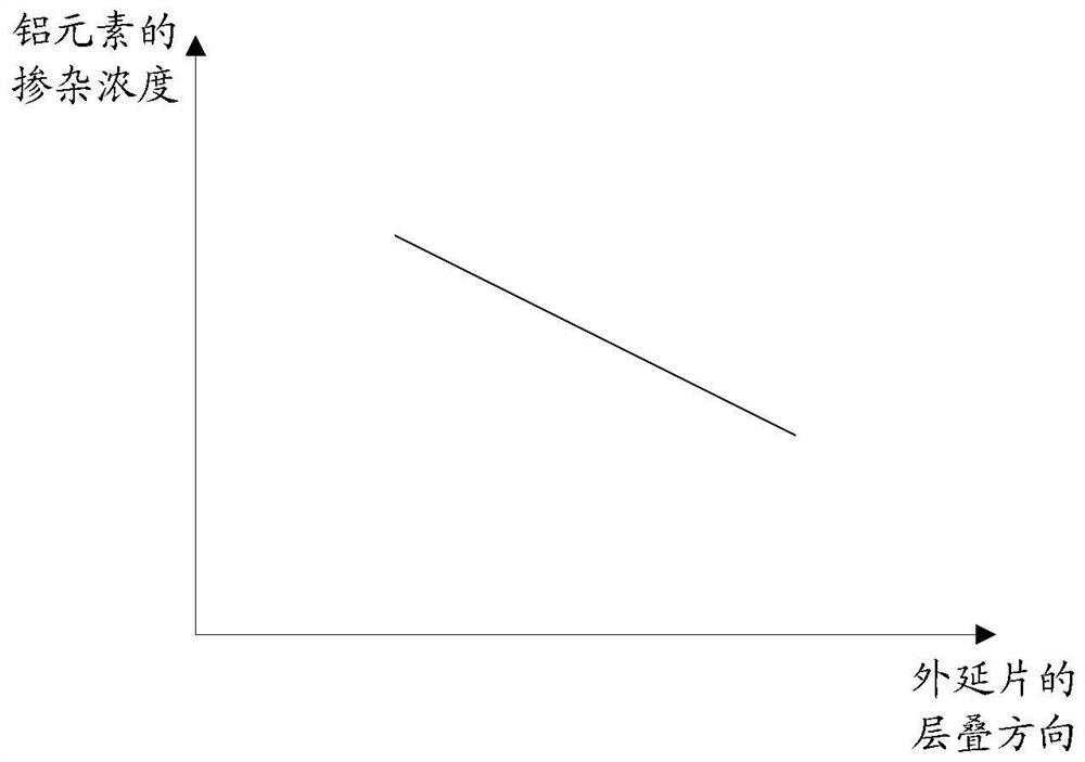
[0031] In this embodiment, the material of the carrier adjustment layer 30 is aluminum indium gallium nitride doped with magnesium.

[0032] In the ...


PUM

PropertyMeasurementUnit
thicknessaaaaaaaaaa
temperatureaaaaaaaaaa
thicknessaaaaaaaaaa

Abstract

The invention discloses a light-emitting diode epitaxial wafer and a preparation method thereof, belonging to the technical field of semiconductors. The light-emitting diode epitaxial wafer includes a substrate, an N-type semiconductor layer, a carrier adjustment layer, an active layer, and a P-type semiconductor layer, and the N-type semiconductor layer, the carrier adjustment layer, the active layer, and the P-type semiconductor layer in sequence Laminated on the substrate, the material of the carrier adjustment layer is aluminum indium gallium nitrogen doped with magnesium. In the present invention, an electron blocking layer with a wide band gap is formed by inserting a magnesium-doped AlInGaN layer between the N-type semiconductor layer and the active layer to avoid electron overflow; at the same time, it provides holes to consume electrons and prolongs the active time of electron injection. Layer time; and the built-in electric field formed in the active layer is reduced, and the hole injection efficiency is improved. In summary, inserting a magnesium-doped AlInGaN layer between the N-type semiconductor layer and the active layer can change the distribution of carriers, so that the number of electrons injected into the active layer matches the number of holes, and ultimately improve the LED performance. luminous efficiency.

Description

technical field [0001] The invention relates to the technical field of semiconductors, in particular to a light-emitting diode epitaxial wafer and a preparation method thereof. Background technique [0002] A light-emitting diode (English: Light Emitting Diode, referred to as: LED) is a semiconductor electronic component that can emit light. Gallium Nitride (GaN)-based LED devices, as a new type of high-efficiency, environmentally friendly and green solid-state lighting source, are often used in traffic lights, outdoor full-color displays, urban landscape lighting, automotive interior and exterior lights, mobile phone backlights, etc. field. [0003] Epitaxial wafers are the primary products in the LED manufacturing process. The existing LED epitaxial wafer includes a substrate, an N-type semiconductor layer, an active layer and a P-type semiconductor layer, and the N-type semiconductor layer, the active layer and the P-type semiconductor layer are sequentially stacked on ...

Claims


Application Information

Patent Timeline
Patent Type & Authority Patents(China)
IPC IPC(8): H01L33/32H01L33/00
CPCH01L33/0066H01L33/0075H01L33/325
Inventor 蒋媛媛印从飞从颖胡加辉李鹏
Owner HC SEMITEK ZHEJIANG CO LTD
Features
  • R&D
  • Intellectual Property
  • Life Sciences
  • Materials
  • Tech Scout
  • Unparalleled Data Quality
  • Higher Quality Content
  • 60% Fewer Hallucinations
Learn More