

Method for detecting sapphire wafer defects
A technology of sapphire wafer and detection method, which is applied in the field of sapphire wafer research, can solve problems such as costing a lot of money and unfavorable industrial production, and achieve the effects of reducing detection errors, facilitating implementation, and simple and easy detection methods
- Summary
- Abstract
- Description
- Claims
- Application Information
AI Technical Summary
Problems solved by technology
Method used
Image

Examples
Embodiment 1
[0035] In the present embodiment, a kind of detection method of sapphire wafer defect is provided, and described detection method comprises:
[0036] (1) 1000 sapphire wafers to be tested are cleaned with a mixture of organic alkali, surfactant and deionized ultrapure water, and dried to obtain a sapphire wafer with a smooth surface;
[0037](2) In a pure water environment, the sapphire wafer with a smooth surface obtained in step (1) is clamped on the fixture with a clamping device, and the position of the sapphire wafer and the light source is adjusted so that the illuminance is 2000Lux and the color of the irradiated light is white LED The soft light is irradiated vertically on the surface of the sapphire wafer with a thickness of 500 μm, and then observed with the naked eye to judge whether the silicon polished wafer is defective.
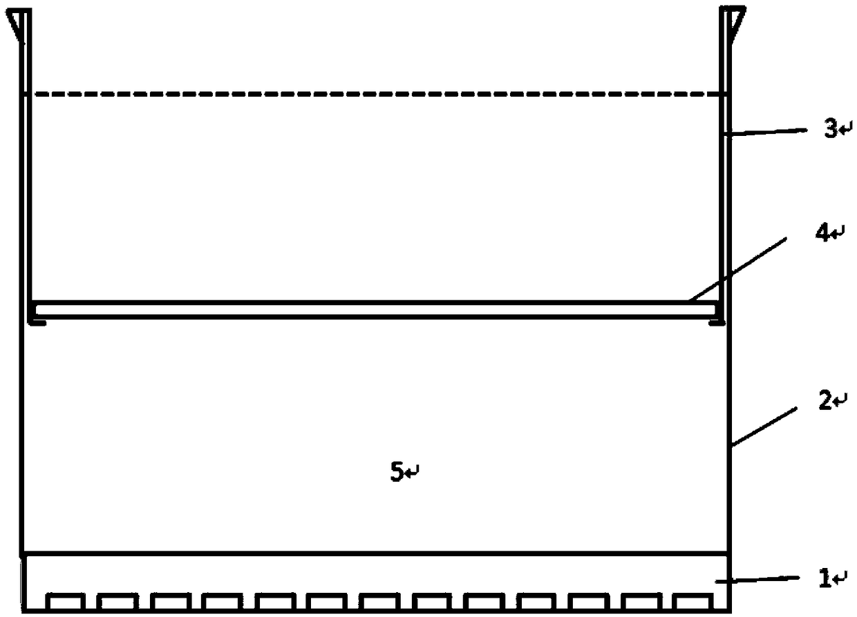
[0038] figure 1 It is a schematic diagram of the structure of the sapphire wafer detection device in this embodiment, wherein: 1 is a light s...
Embodiment 2
[0042] In the present embodiment, a kind of detection method of sapphire wafer defect is provided, and described detection method comprises:
[0043] (1) 1000 sapphire wafers to be tested are cleaned with a mixture of organic alkali, surfactant and deionized ultrapure water, and dried to obtain a sapphire wafer with a smooth surface;
[0044] (2) In a pure water environment, the sapphire wafer with a smooth surface obtained in step (1) is clamped on the fixture with a clamping device, and the position of the sapphire wafer and the light source is adjusted so that the illuminance is 1500Lux and the color of the irradiated light is a yellow LED The soft light is irradiated vertically on the surface of the sapphire wafer with a thickness of 700 μm, and then observed with the naked eye to judge whether the silicon polished wafer is defective.
[0045] Visual observation: Among the 1000 sapphire wafers to be tested, 66 sapphire wafers had air bubbles, micro-cracks, clouds and growt...
Embodiment 3
[0048] In the present embodiment, a kind of detection method of sapphire wafer defect is provided, and described detection method comprises:
[0049] (1) 1000 sapphire wafers to be tested are cleaned with a mixture of organic alkali, surfactant and deionized ultrapure water, and dried to obtain a sapphire wafer with a smooth surface;
[0050] (2) In a pure water environment, the sapphire wafer with a smooth surface obtained in step (1) is clamped on the fixture with a clamping device, and the position of the sapphire wafer and the light source is adjusted so that the illuminance is 3000 Lux and the color of the irradiated light is yellow. The LED soft light is irradiated vertically on the surface of the sapphire wafer with a thickness of 300 μm, and then observed with the naked eye to judge whether the sapphire wafer is defective.
[0051] Visual observation: Among the 1000 sapphire wafers to be tested, 66 sapphire wafers had air bubbles, micro-cracks, clouds and growth lines,...
PUM
| Property | Measurement | Unit |
|---|---|---|
| thickness | aaaaa | aaaaa |
| refractive index | aaaaa | aaaaa |
Abstract
Description
Claims
Application Information