
Method for forming graphene film, MEMS microphone and forming method thereof

A graphene film and microphone technology, applied in gaseous chemical plating, coatings, electrical components, etc., can solve problems such as breakage and graphene film cracking, and achieve the effect of saving costs and reducing the risk of cracking or breakage

Active Publication Date: 2019-02-26
SEMICON MFG INT (SHANGHAI) CORP +1
View PDF2 Cites 3 Cited by
  • Summary
  • Abstract
  • Description
  • Claims
  • Application Information

AI Technical Summary

Problems solved by technology

[0005] The object of the present invention is to provide a kind of forming method of graphene film, to improve the problem that graphene film cracks or breakage occurs

Method used


Image

  • Method for forming graphene film, MEMS microphone and forming method thereof
  • Method for forming graphene film, MEMS microphone and forming method thereof
  • Method for forming graphene film, MEMS microphone and forming method thereof

Examples


Embodiment Construction

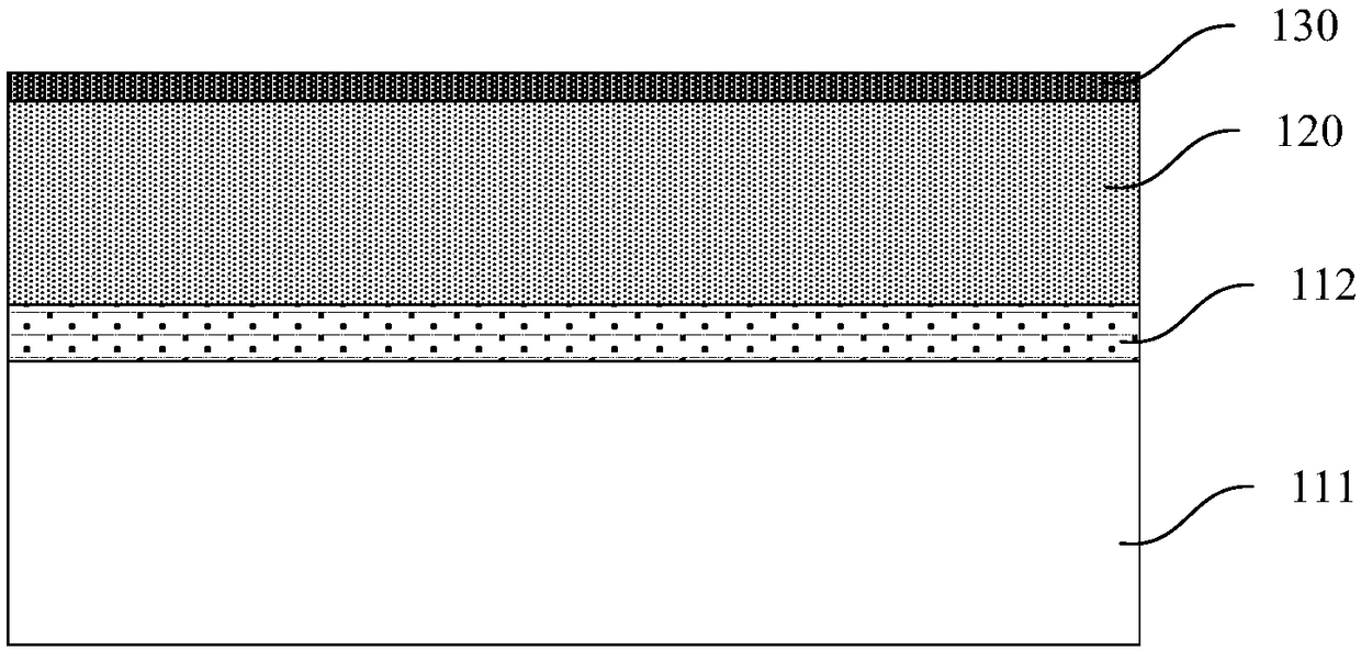
[0036] Graphene has great application prospects due to its excellent properties in mechanics, electricity, optics and chemistry. However, when it is necessary to form a graphene film on a specific substrate, it is usually necessary to provide a transition substrate, and the graphene film is formed on the transition substrate, and then the graphene film formed is transferred to the specific substrate. Like this, not only make the transfer process of graphene film comparatively loaded down with trivial details, and also easily cause the cracking or breakage of graphene film.

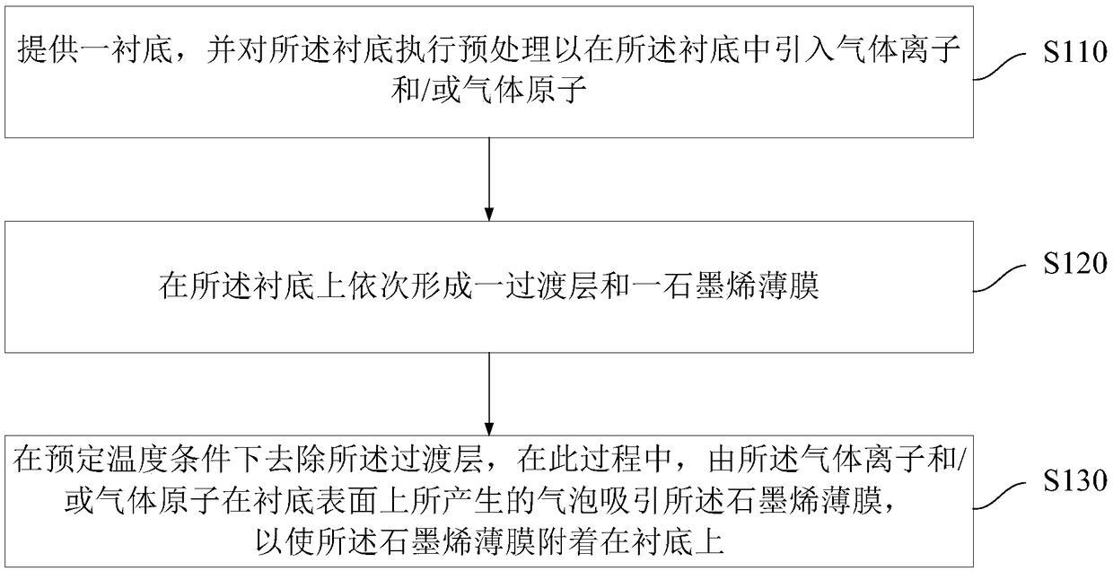
[0037] To this end, the invention provides a method for forming a graphene film. figure 1 It is a schematic flow diagram of a method for forming a graphene layer in Embodiment 1 of the present invention, as figure 1 Shown, the formation method of described graphene layer comprises:

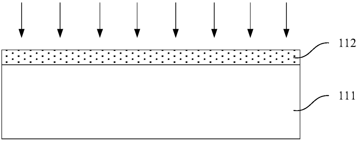
[0038] Step S110, providing a substrate, and performing pretreatment on the substrate to introduce gas ions and / or gas ato...


PUM


Abstract

The invention provides a method for forming a graphene film, a MEMS microphone and a forming method thereof. The method comprises the following steps: introducing gas ions and / or gas atoms into a substrate; sequentially forming a transition layer and the graphene film on the substrate; absorbing the graphene film by the bubbles generated by the gas atoms and / or the gas atoms on the surface of thesubstrate during the process of removing the transition layer, and attaching the graphene film on the substrate. According to the forming method provided by the present invention, the graphene film can be formed on the target substrate without additionally providing a transition substrate, and the cost can be effectively saved; the graphene film is attracted by the bubbles, and the capillary channel inside is spontaneously bridged with the bubbles and adsorbed on the substrate, so that the risk of cracking or breakage of the graphene film can be effectively reduced.

Description

technical field [0001] The invention relates to the field of semiconductor technology, in particular to a method for forming a graphene film, a MEMS microphone and a method for forming the same. Background technique [0002] Graphene is a nanostructure with a two-dimensional honeycomb, which has high electron mobility, Young's modulus, and thermal conductivity, and has attracted great interest from researchers in various fields. For example, it has broad application prospects in many fields such as electronic devices, transparent electrode materials, and energy storage materials. [0003] In order to realize various potential applications of graphene, it is usually necessary to form graphene films on specific substrate surfaces, such as silicon substrates or silicon-silicon oxide substrates. In addition, the chemical vapor deposition process has become an important means of forming graphene films because of its advantages of large-scale production and the ability to grow hi...

Claims


Application Information

Patent Timeline
Patent Type & Authority Applications(China)
IPC IPC(8): C23C16/26C23C16/02C23C16/01H04R19/04H04R31/00
CPCC23C16/01C23C16/0281C23C16/26H04R19/04H04R31/00
Inventor 李鑫王伟周鸣
Owner SEMICON MFG INT (SHANGHAI) CORP
Learn More