
Novel wide band gap semiconductor device and manufacturing method thereof

A power semiconductor and wide bandgap technology, applied in the field of new wide bandgap power semiconductor devices and their production, can solve the problems of miniaturization and high power density of power electronic equipment, high conduction voltage drop of MOS body diode, and increase of equipment volume. and cost to improve conduction loss characteristics, reduce system size and parasitic parameters, and improve the effect of peak electric field

Pending Publication Date: 2019-02-26
XIDIAN UNIV +1
View PDF0 Cites 0 Cited by
  • Summary
  • Abstract
  • Description
  • Claims
  • Application Information

AI Technical Summary

Problems solved by technology

[0004] However, silicon carbide MOS devices also have corresponding disadvantages. Due to its wide bandgap, its MOS body diode conduction voltage drop is high, and when it works in reverse, the loss is large, and the traditional method is reversed and low conduction voltage drop in power electronic devices. SiC Schottky diode, improve its reverse freewheeling capability and reduce loss
But doing so increases the volume and cost of the equipment, which is not conducive to the miniaturization and high power density of power electronic equipment

Method used


Image

  • Novel wide band gap semiconductor device and manufacturing method thereof
  • Novel wide band gap semiconductor device and manufacturing method thereof
  • Novel wide band gap semiconductor device and manufacturing method thereof

Examples


Embodiment Construction

[0031] In order to deepen the understanding and recognition of the present invention, the present invention will be further described and introduced below in conjunction with the accompanying drawings.

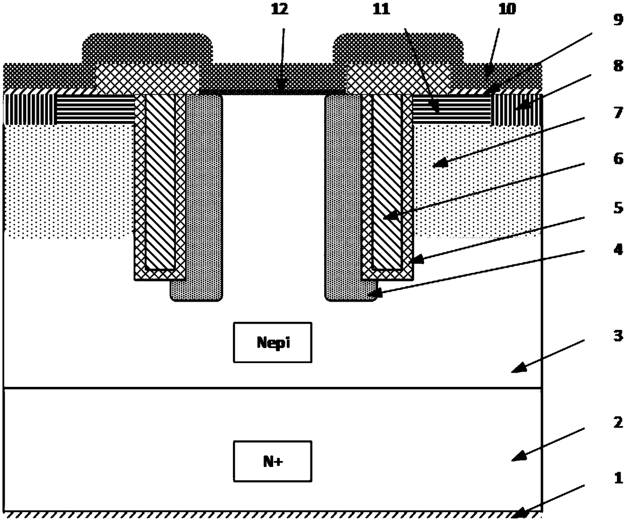
[0032] Such as figure 1 As shown, a new wide-bandgap power semiconductor device includes an N+ substrate 2, an N-type epitaxial layer 3 deposited on the N+ substrate 2, a PWELL region 7 (ie, a P well region) located inside the epitaxial layer, and a set The N+ implantation region 11 and the P+ implantation region 8 in the P well region, the plurality of trenches arranged inside the P well region, the ohmic contact electrode 9 arranged on the top of the N+ implantation region 11 and the P+ implantation region 8, and the grooves The P-type doped layer 4 on one side, the Schottky contact electrode 12 arranged on the top between the P-type doped layers 4, the groove extends toward the substrate, and the POLY gate 6 is filled in the groove, and the POLY gate 6 The oxide layer 5 th...


PUM


Abstract

The invention relates to a novel wide band gap semiconductor device and a manufacturing method thereof. The device comprises the components of a first conductive type substrate, a first conductive type epitaxial layer deposited on the substrate, a first well region and a second well region in the epitaxial layer, a second conductive type region in the first well region and the second well region,a first conductive type implantation region and a second conductive type implantation region in the first and the second well regions, a plurality of grooves arranged at inner side of the first well region and the second well region, ohmic contact electrodes arranged at the upper part of the first conductive type implantation region and the second conductive type implantation region, a second conductive type doping layer arranged at one side of the groove, and a Schottky contact electrode which is arranged at top between the second conductive type doping layers. A POLY gate is arranged in thegroove. The surrounding part of the POLY gate is provided with an oxide layer which can wrap the POLY gate. The back of the first conductive type substrate is provided with a back electrode. Front electrodes are arranged at top of the ohmic contact electrode, the Schottky contact electrode and a passivation layer. The novel wide band gap semiconductor device has advantages of low reverse loss andhigh freewheeling capability.

Description

technical field [0001] The invention relates to the technical field of power semiconductor devices, in particular to a novel wide-bandgap power semiconductor device and a manufacturing method thereof. Background technique [0002] With the rapid development of global science and technology, higher requirements are put forward for power electronic devices in the fields of aerospace, nuclear technology, energy, and communication, requiring them to have small size, light weight, high conversion efficiency, high temperature and high reliability, etc. High-performance, traditional silicon-based devices have been difficult to meet the above requirements, new materials, high-performance power semiconductor devices with new structures need to be developed urgently, and silicon carbide, a semiconductor material with a wide bandgap, has a large bandgap width and a high saturation drift speed Excellent characteristics such as high breakdown electric field strength and high thermal cond...

Claims


Application Information

Patent Timeline
Patent Type & Authority Applications(China)
IPC IPC(8): H01L27/06H01L29/872H01L21/8234
CPCH01L27/0629H01L29/872H01L21/8234
Inventor 李鹏颜剑谭在超丁国华罗寅张玉明
Owner XIDIAN UNIV
Learn More