OLED device

A technology of devices and nanomaterials, applied in the field of QLED devices, can solve problems such as high lighting voltage, device luminescence quenching, and poor stability, and achieve the effects of reducing driving voltage, reducing quenching, and long service life

Inactive Publication Date: 2019-02-26
TCL CORPORATION
View PDF6 Cites 1 Cited by
  • Summary
  • Abstract
  • Description
  • Claims
  • Application Information

AI Technical Summary

Problems solved by technology

[0004] The purpose of the present invention is to provide a QLED device, aiming to solve the problem of high lighti

Method used


Image

  • OLED device
  • OLED device
  • OLED device

Examples


Embodiment 1

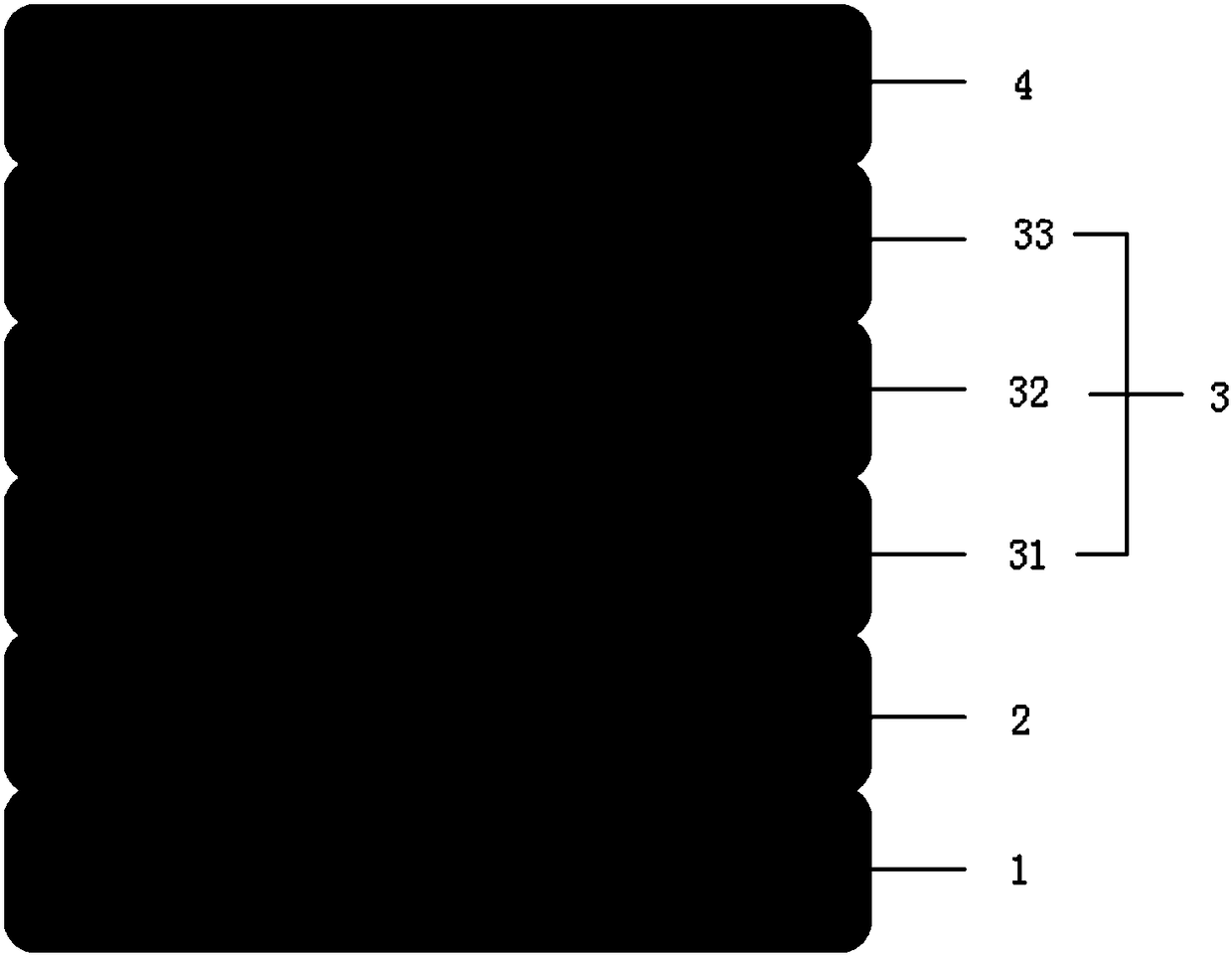
[0038] A QLED device, comprising a bottom electrode, a bipolar Auger energy multiplication structure and a top electrode sequentially stacked on a glass substrate, the bipolar Auger energy multiplication structure is a sequentially combined hole transport layer, quantum dot light emitting Layer and electron transport layer, wherein, the substrate is a glass substrate, the anode is 120nm ITO, the electron transport layer is nickel oxide with a size of 5nm and a thickness of 25nm, and the quantum dot light-emitting layer is 40nm CdSe / ZnS (luminescence wavelength 530 nm, quantum yield 90%), the hole transport layer is zinc oxide with a size of 3 nm and a thickness of 20 nm, and the cathode is Al.

Embodiment 2

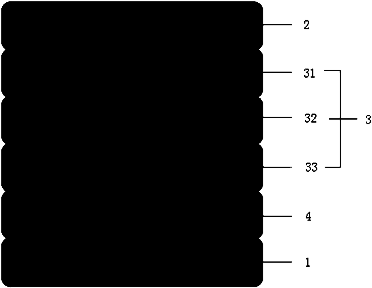
[0040] A QLED device, comprising a bottom electrode, a bipolar Auger energy multiplication structure and a top electrode sequentially stacked on a glass substrate, the bipolar Auger energy multiplication structure is a sequentially combined hole transport layer, quantum dot light emitting Layer and electron transport layer, wherein, the substrate is a glass substrate, the anode is 120nm ITO, the electron transport layer is copper-doped nano-molybdenum oxide with a thickness of 50nm, and the doped nano-molybdenum oxide The size is 10nm, the doping weight percentage of copper is 10%, the quantum dot light-emitting layer is 40nm CdSe / ZnS (luminescence wavelength 632 nanometers, quantum yield 85%), and the hole transport layer is It is 20nm lithium-doped nano-zinc oxide, and the size of the doped nano-zinc oxide is 3nm, the doping weight percentage of lithium is 5%, and the cathode is Al.

Embodiment 3

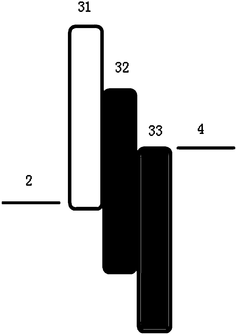
[0042] A QLED device, comprising a bottom electrode, a bipolar Auger energy multiplication structure and a top electrode sequentially stacked on a glass substrate, the bipolar Auger energy multiplication structure is a sequentially combined hole transport layer, quantum dot light emitting Layer and electron transport layer, wherein, the substrate is a glass substrate, the anode is 120nm ITO, the electron transport layer is copper-doped nano-molybdenum oxide with a thickness of 30nm, and the doped nano-molybdenum oxide The size is 5nm, the doping weight percentage of copper is 10%, the quantum dot light-emitting layer is 40nm CdSe / ZnS (light-emitting wavelength 530 nanometers, quantum yield 90%), and the hole transport layer is It is 20nm aluminum-doped nano-zinc oxide, and the size of the doped nano-zinc oxide is 3nm, the doping weight percentage of lithium is 5%, and the cathode is Al.


PUM

PropertyMeasurementUnit
Mobilityaaaaaaaaaa
Sizeaaaaaaaaaa
Thicknessaaaaaaaaaa

Abstract

The present invention provides a QLED device comprising a bottom electrode, a bipolar Auger energy multiplying structure and a top electrode, wherein the bottom electrode, a bipolar Auger energy multiplying structure and the top electrode are sequentially laminated on a substrate, and the bipolar Auger energy multiplying structure comprises a hole transport layer, a quantum dot light-emitting layer and an electron transport layer, and the hole transport layer, the quantum dot light-emitting layer and the electron transport layer are sequentially bonded. The electron transport layer is made ofan n-type nano material, and the hole transport layer is made of a p-type nano material.

Description

technical field [0001] The invention belongs to the technical field of light emitting diodes, in particular to a QLED device. Background technique [0002] The quantum confinement effect makes the luminous quantum dots at the nanometer scale, and its luminous color can be adjusted with the size, especially for 2-6 group semiconductor materials, the entire visible spectrum (from red light to to blue light) continuously adjustable illuminance. Compared with organic light-emitting materials, quantum dots also have the advantages of higher resistance to water and oxygen. Based on this, quantum dot-based light-emitting diodes (QLEDs) have the advantages of high color purity, continuously adjustable luminous color, and good resistance to water and oxygen. In addition, QLED also has the characteristics of thinness and flexibility of organic light-emitting diodes (OLEDs), so it has very good application prospects in the display field. Although QLED shows a good application prospe...

Claims


Application Information

Patent Timeline
IPC IPC(8): H01L33/06H01L33/26H01L33/28B82Y30/00B82Y20/00
CPCB82Y20/00B82Y30/00H01L33/06H01L33/26H01L33/285
Inventor 钱磊杨一行曹蔚然向超宇陈崧
Owner TCL CORPORATION
Why Eureka
Try Eureka