Method for electrolytic deposition of WO3 thin film on non-continuous conducting film

A technology of conductive film and electrodeposition, which is applied in the direction of non-woven fabrics, plating of superimposed layers, electrolytic inorganic material plating, etc., can solve the problems of high cost of preparation methods, achieve low cost, large control window, and cost saving effects

Active Publication Date: 2019-03-01
XIAMEN UNIV +1
View PDF4 Cites 2 Cited by
  • Summary
  • Abstract
  • Description
  • Claims
  • Application Information

AI Technical Summary

Problems solved by technology

[0016] The purpose of the present invention is to address the serious limitations of current electrochromic devices in terms of flexible electronics and the currently reported WO 3 The problem of high cost of the preparatio

Method used


Image

  • Method for electrolytic deposition of WO3 thin film on non-continuous conducting film
  • Method for electrolytic deposition of WO3 thin film on non-continuous conducting film
  • Method for electrolytic deposition of WO3 thin film on non-continuous conducting film

Examples


Embodiment 1

[0042] (1) figure 1 It is a schematic structural diagram of the W / Ag NTs / W / PET transparent conductive film of the present invention. Cut a commercially available PET (or other flexible substrate) flexible film (light transmittance ~ 95%) with a thickness of 100 μm into small rectangular pieces, and ultrasonically clean the PET surface with ethanol and water respectively, and use it as a substrate for future use. Then fix it in the chamber of the magnetron sputtering instrument, pass in argon gas, set the sputtering parameters as pressure 4-6Pa, power 60-100W, sputtering time 1-10min for WO 3 Sputtering of the base layer.

[0043] (2) PVA nanofibers were prepared by electrospinning, and the grooves made of thick aluminum foil were used as PVA spinning receivers. The PVA solution is used as the spinning ink, and the spinning is carried out perpendicular to the groove in an electric field with a positive voltage of 10-15kV and a negative voltage of 0-2kV. The obtained nanofibe...

Embodiment 2

[0048] Step (1), (2) are identical with embodiment 1.

[0049] (3) H with a ratio of 1:4:50 2 o 2 : HClO 4 : DI water is added into the beaker and mixed to obtain the deposition solution. Put the conductive substrate obtained in step (3) into the deposition solution, and set the parameters on the electrochemical workstation to deposit WO 3 , the pulse voltage of each cycle is: -1V, 0.1s, 0V, 0.5s and the cycle interval of 1.1 ~ 1.5s. Set the total deposition time to 1.5 h. From Figure 7 It can be seen that as the deposition time increases, the discoloration window of the film increases to 80.6%.

[0050] (4) This step is the same as step (4) in Example 1.

[0051] The discoloration window test curve of the sample prepared in the embodiment of the present invention 2 sees Figure 6 .

Embodiment 3

[0053] Steps (1) and (2) are the same as in Example 1.

[0054] (3) H with a ratio of 1:4:50 2 o 2 : HClO 4 : DI water is added into the beaker and mixed to obtain the deposition solution. Put the conductive substrate obtained in step (3) into the deposition solution, and set the parameters on the electrochemical workstation to deposit WO 3 , the pulse voltage of each cycle is: -1V, 0.1s, 0V, 0.5s and the cycle interval of 1.1 ~ 1.5s. Set the total deposition time to 2h. From Figure 8 It can be seen that as the deposition time increases, the film thickness increases, and the discoloration window of the film increases to 89.7%.

[0055] (4) This step is the same as step (4) in Example 1.

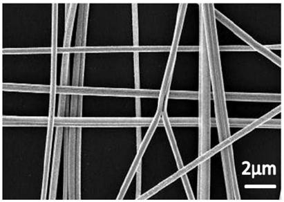
[0056] The discoloration window test curve of the sample prepared in the embodiment of the present invention 3 sees Figure 7 , the SEM of the different magnifications of the sample prepared in the embodiment of the present invention 3 sees Figure 8 .


PUM


Abstract

The invention discloses a method for electrolytic deposition of a WO3 thin film on a non-continuous conducting film, and relates to the technology of functional materials. A magnetron sputtering technology is utilized for sputtering WO3 on the surface of a PET thin film to obtain a WO3/PET film; a PVA nano fiber net is obtained through electrostatic spinning, metallic silver coating is formed on the surface of the PVA nano fiber net, a PVA template is removed to obtain a nano groove conducting grid, and then the conducting grid is transferred to the obtained WO3/PET film to obtain a compound thin film; a WO3 top-level layer is subjected to magnetron sputtering on the compound thin film to form a transparent conducting substrate of a sandwich structure; an electrochemical deposition methodis adopted for preparing a WO3 color changing layer on the transparent conducting substrate of the sandwich structure, and the electrolytic deposition of the WO3 thin film on the non-continuous conducting film is completed. According to the method, the cost is reduced, and the high-transmittance non-continuous conducting film is applied to the electrochemical deposition method.

Description

technical field [0001] The present invention relates to functional material technology, especially to flexible WO 3 A sandwich-based electrodeposition of color-changing electrodes on discontinuous conductive films of WO 3 thin film method. Background technique [0002] So far, there are many 3 research reports, especially in the field of electrochromic (EC) research. Due to the low power consumption, high coloring efficiency, and stable memory effect, EC devices have broad application prospects in building smart windows, rearview mirrors, digital displays, etc. However, the continuous development of modern electrochromic devices not only escalates the need for advanced fabrication techniques, but also emphasizes the high quality of electrochromic films and their versatility. In order to meet the development trend of modern electronic products, high-quality electrochromic films need to have the following advantages, such as large optical modulation, short switching time a...

Claims


Application Information

Patent Timeline
IPC IPC(8): C23C14/04C23C14/35C25D5/18C25D9/04D04H1/4309D04H1/728C23C28/04
CPCC23C14/042C23C14/35C23C28/042C25D5/18C25D9/04D04H1/4309D04H1/728
Inventor 郭文熹王亚楠李戌一李艳冉刘向阳
Owner XIAMEN UNIV
Why Eureka
Try Eureka