Two-dimensional bismuth oxygen selenium atom crystal materials and preparation method and application thereof

A crystal material, bismuth oxide technology, applied in the field of two-dimensional materials, can solve the problem that the ratio of bismuth source and selenium source is not easy to control, and achieve the effect of large area growth, low preparation cost and high purity

Active Publication Date: 2019-03-01
TSINGHUA BERKELEY SHENZHEN INST
View PDF7 Cites 15 Cited by
  • Summary
  • Abstract
  • Description
  • Claims
  • Application Information

AI Technical Summary

Problems solved by technology

[0010] The invention adopts physical vapor deposition, which solves the problem that the ratio of bismuth source and selenium source is not easy to control in the process of chemical vapor phase reaction, and the obtained two-dimensional bismuth oxygen selenium atomic crystal material has higher purity, fewer vacancy defects, and further, electron mobility Higher, electron mobility ≥ 135cm 2 /(V s)

Method used


Image

  • Two-dimensional bismuth oxygen selenium atom crystal materials and preparation method and application thereof
  • Two-dimensional bismuth oxygen selenium atom crystal materials and preparation method and application thereof
  • Two-dimensional bismuth oxygen selenium atom crystal materials and preparation method and application thereof

Examples


Embodiment 1

[0064] A preparation method of a two-dimensional bismuth oxyselenide atomic crystal material comprises the following steps:

[0065] Bi 2 o 2 Se powder is placed in the upstream end area of ​​the airflow direction of the horizontal tube furnace, and the mica substrate is placed in the downstream end area of ​​the reaction furnace in the airflow direction, Bi 2 o 2 The distance between the Se powder and the mica substrate is 6 cm, and the temperature rises to 620 °C at a rate of 30 °C / min in a nitrogen gas environment. 2 o 2 The Se powder was heat-treated for 25 minutes. After the heat treatment, the reaction system was naturally cooled to 25°C under the condition of a nitrogen gas flow rate of 200 sccm, and the test results of the two-dimensional bismuth oxygen selenium atomic crystal material were as follows: Figure 1-12 shown.

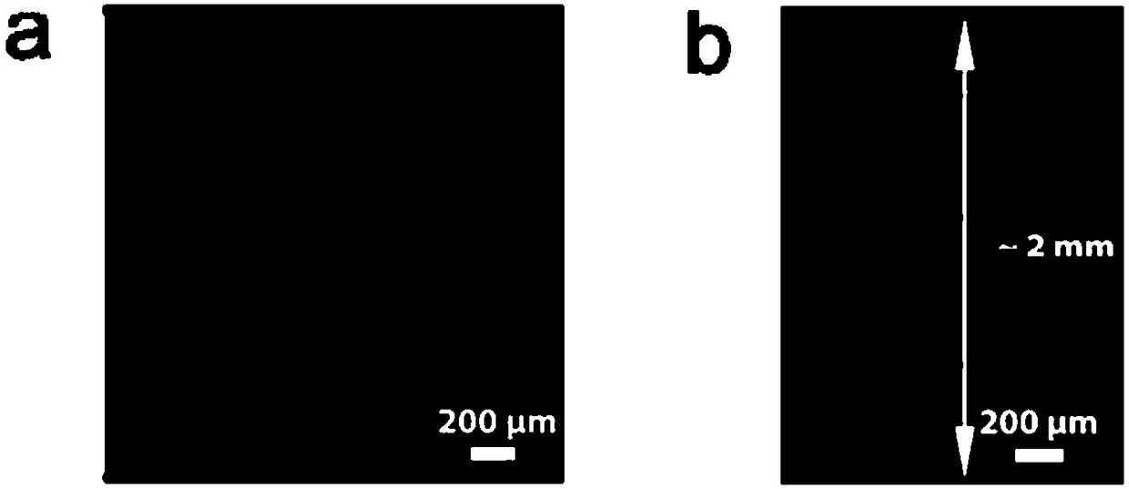
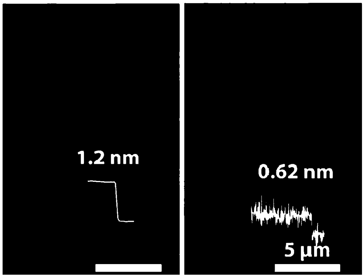
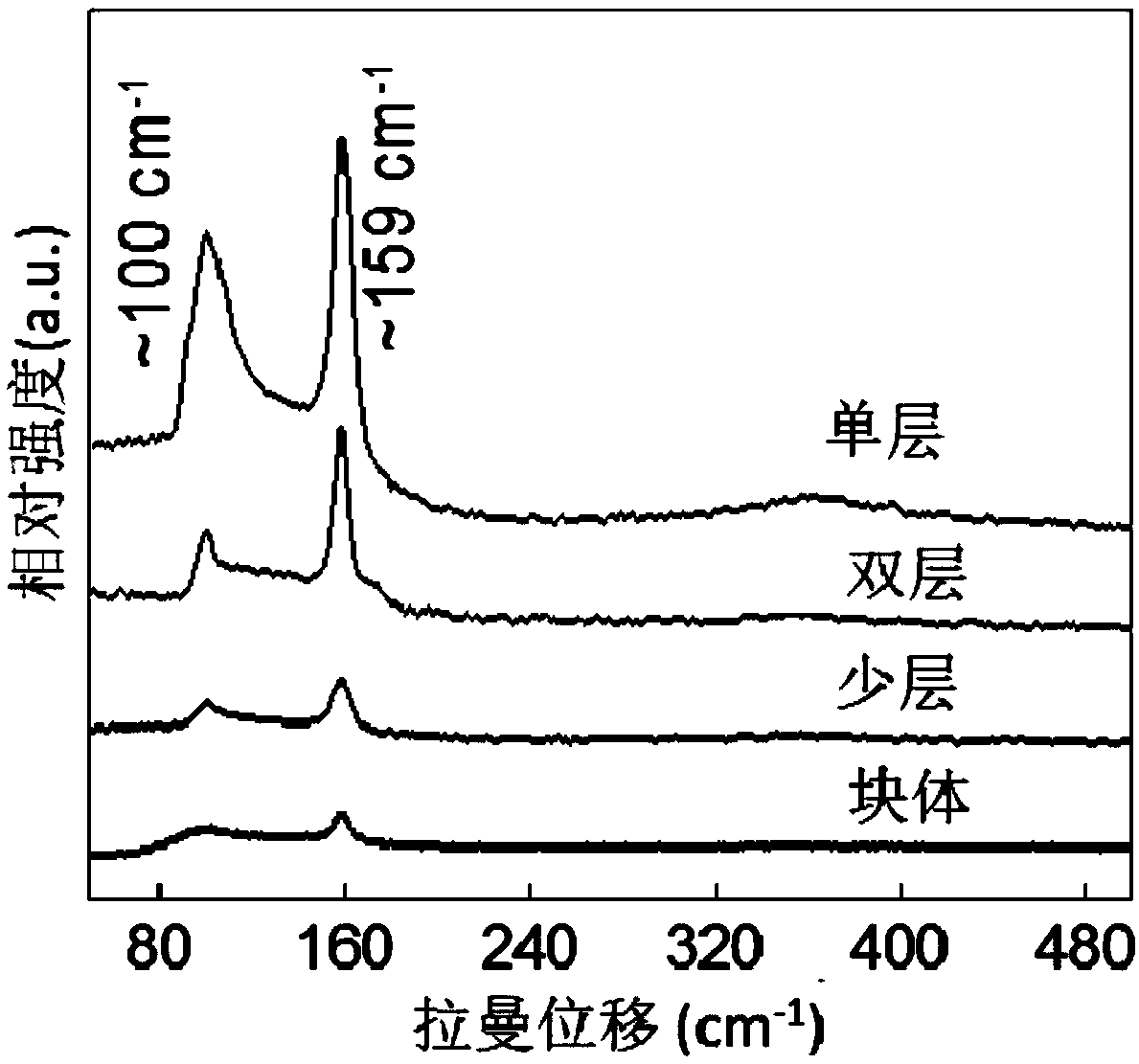
[0066] figure 1 a, 1b are optical microscope pictures of the two-dimensional bismuth oxygen selenium atomic crystal material prepared by fig...

Embodiment 2

[0079] The difference from Example 1 is that the heat treatment temperature is 580°C.

Embodiment 3

[0081] The difference from Example 1 is that the heat treatment temperature is 800°C.


PUM

PropertyMeasurementUnit
Electron mobilityaaaaaaaaaa

Abstract

The invention relates to a preparation method of two-dimensional bismuth oxygen selenium atom crystals. The method comprises the following steps that a precursor containing bismuth elements and selenium elements is subjected to physical vapor deposition, a two-dimensional bismuth oxygen selenium atom crystal material is obtained, and the two-dimensional bismuth oxygen selenium atom crystal material is a tetragonal system. By adopting physical vapor deposition, the problem that the ratio of a bismuth source to a selenium source is not easily controlled in the chemical gas-phase reaction processis solved, the obtained two-dimensional bismuth oxygen selenium atom crystal material is higher in purity, vacancy defects are less, then, the electronic mobility is higher, the electronic mobility is larger than or equal to 135 cm<2>/(V s), meanwhile, compared with chemical vapor deposition, the physical vapor deposition can enable the crystal form integrity of the two-dimensional bismuth oxygenselenium atom crystal material to be higher, the crystal size is larger, the single crystal domain edge can reach the millimeter scale, the maximum single crystal domain edge is not smaller than 1.7mm, and the minimum signed crystal domain edge is not smaller than 200 micrometers.

Description

technical field [0001] The invention belongs to the field of two-dimensional materials, and in particular relates to a two-dimensional bismuth oxygen selenium atomic crystal material, its preparation method and application. Background technique [0002] The progress of modern information technology depends to a large extent on the development of integrated circuits based on semiconductor silicon. At present, due to the limitations of physical laws such as short channel effects and manufacturing costs, the mainstream CMOS (complementary metal oxide semiconductor) technology is about to reach the 10nm technology node, and it is difficult to continue to improve, which also indicates that "Moore's Law" may face end. Therefore, exploring new channel materials and transistor technology with new principles in order to replace silicon-based CMOS technology has always been one of the mainstream research directions in the scientific and industrial circles. [0003] At the same time,...

Claims


Application Information

Patent Timeline
IPC IPC(8): C30B29/46C30B29/64C30B23/00H01L29/24H01L31/032
CPCH01L29/24H01L31/032C30B23/00C30B29/46C30B29/64
Inventor 成会明乌斯曼·汗唐磊罗雨婷刘碧录
Owner TSINGHUA BERKELEY SHENZHEN INST
Why Eureka
Try Eureka