P well/inversely doped deep N well CMOS SPAD photoelectric device

An optoelectronic device and reverse doping technology, applied in the field of photoelectric detection, can solve problems such as increasing dark counts, and achieve the effect of improving detection efficiency

CN109411550AInactive Publication Date: 2019-03-01重庆亚川电器有限公司
4 Cites 1 Cited by

Patent Information

Authority / Receiving Office
CN · China
Current Assignee / Owner
Publication Date
2019-03-01
Estimated Expiration
Not applicable · inactive patent

Smart Images

  • Figure 1
    Figure 1
  • Figure 2
    Figure 2
  • Figure 3
    Figure 3
Patent Text Reader

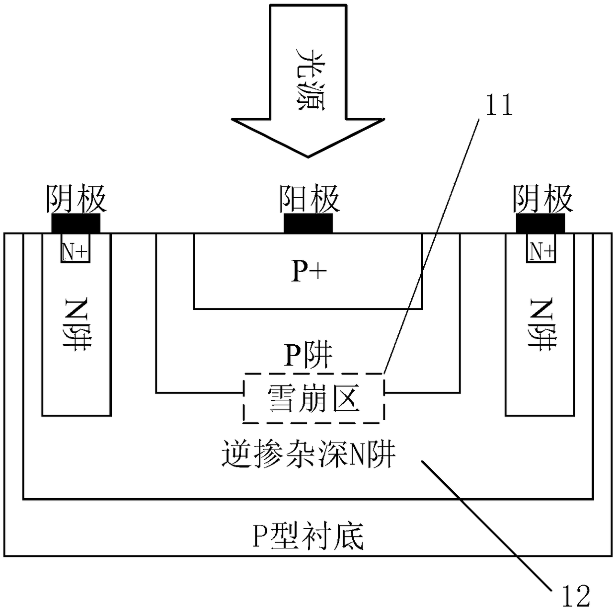
Abstract

The invention provides a P well / inversely doped deep N well CMOS SPAD photoelectric device. The device is of a plane structure of a P+ / P well / inversely doped deep N well / P substrate; compared with a conventional SPAD device, the two aspects of the dark counting rate and the photon detection efficiency are improved. The device adopts a P well layer instead of a traditional P+ layer as an anode, while the contact position of P well and inversely doped deep N well forms a main working region of the device to be used for detecting photons; and meanwhile, the inversely doped deep N well serves as avirtual protection ring and a photon absorption region of the device. In addition, the inversely doped deep N well serves as a main photon absorption region of the device, so that most of the incident photons can be used by the device to form the optical current, and therefore the photon detection efficiency of the device is improved. A single-photon avalanche diode with low dark counting rate and high photon detection efficiency is designed from two aspects of changing the PN junction type of the device and increasing the thickness of the photon absorption region of the device.
Need to check novelty before this filing date? Find Prior Art

Description

technical field

[0001] The invention belongs to the technical field of photoelectric detection, specifically the technical field of single photon detection, and relates to the structural design of an APD optoelectronic device, in particular to the design of a CMOS SPAD optoelectronic device with a new structure having a P well / reversedly doped deep N well. Background technique

[0002] A single photon avalanche diode is a PN junction that works above the avalanche breakdown voltage. In this working mode, the electron-hole pairs are impacted and ionized by the high electric field in the space charge region, so that the output of the device The port forms a detectable current pulse signal. Because of this characteristic, single photon avalanche diodes are widely used in 3D imaging, biophotonics, fluorescence lifetime imaging and other technical fields.

[0003] CMOSSPADs are typically designed and fabricated using a dedicated CMOS process to achieve well-controlled characteri...

Examples

Embodiment Construction

[0018] The technical solutions in the embodiments of the present invention will be described clearly and in detail below with reference to the drawings in the embodiments of the present invention. The described embodiments are only some of the embodiments of the invention.

[0019] The technical scheme that the present invention solves the problems of the technologies described above is:

[0020] Such as figure 1 Shown is a schematic diagram of the structure of the new CMOS SPAD optoelectronic device. Depend on figure 1 It can be seen that the device is a planar structure composed of P+ / P well / reversely doped deep N well / P substrate. Among them, the P-well layer and the counter-doped deep N-well layer constitute the avalanche region of the device (corresponding to position 11 in the figure), and the photogenerated carriers are impacted and ionized by the strong electric field in this region, and further carriers undergo formation times, thus forming a visible current pulse...