

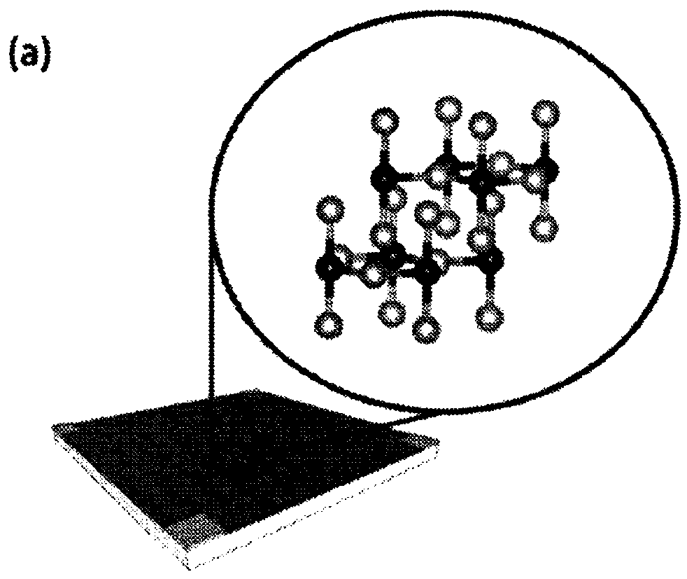
Dirac semimetal structure
A semi-metal and alkali metal technology, applied in the fields of semiconductor devices, semiconductor/solid-state device manufacturing, electrical components, etc., can solve problems such as the useful structure of Dirac semi-metal layers that have not yet been reported
- Summary
- Abstract
- Description
- Claims
- Application Information
AI Technical Summary
Problems solved by technology
Method used
Image

Examples
Embodiment 1
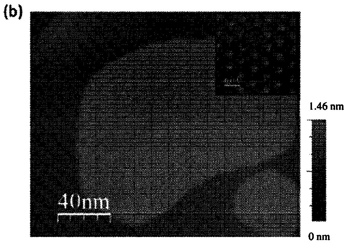
[0071] This example shows that in insulating Al 2 o 3 Form high-quality c-axis orientation film Na on the substrate 3 Bi. It will be appreciated that a number of different substrates can be chosen to form Na 3 Bi Dirac semimetal layer. However, in this case and as mentioned above, using insulating Al 2 o 3 is advantageous because it allows the analysis of Na in a controlled manner without a conductive layer 3 The nature of Bi.
[0072] Films were grown using a two-step method according to an embodiment of the invention. Briefly, a thin (2 nm) nucleation layer was deposited at low (120°C) temperature under simultaneous Bi and Na flux, followed by additional growth at a higher final temperature between 250°C and 390°C. The resulting films were subsequently characterized in situ in ultrahigh vacuum (UHV) using low-temperature magnetic transport and scanning tunneling microscopy and spectroscopy (STM and STS).
[0073] In order to form the film, the Al 2 o 3 [0001] The ...
Embodiment 2
[0094] Fig. 4(a) and Fig. 4(b) show the stencil mask 17 and the prepared substrate structure 10 used in the embodiment of the present invention. The substrate structure 10 includes a sample plate 11 . An insulating substrate is applied thereon to electrically insulate the created structure. Next, a back gate electrode 14 is provided, on top of which Si:SiO 2 substrate.
[0095] Deposit Ti / Au contacts (5 / 50nm) 18 through stencil mask 17 to Si:SiO with 1 μm oxide thickness 2 16. Solvent clean the sheet on the substrate sheet. A stencil mask 17 in the Hall stripe pattern was attached to the substrate surface, and the electrode leads were subsequently bonded to the contact bus bars on the sample board. The substrates were introduced into the UHV immediately after wire bonding to minimize exposure to ambient conditions, and then annealed at 450 °C for 90 min to remove adsorbed atmospheric species.
[0096] Elemental Bi (99.999%, Alfa Aesar) in the flux of Na (99.95%, Sigma Ald...
Embodiment 3
[0100] This example reports an ultrathin topological Dirac semimetal with controlled Na 3 The results related to the band gap of Bi.
[0101] Ultra-thin Na 3 Bi film in ultra-high vacuum (UHV) (10 -10 Torr) in a molecular beam epitaxy (MBE) chamber, and then transferred to a UHV (10 -11 Interconnect Createc LT-STM operated in Torr) for STM / STS measurements at 5K. for Na 3 A Bi film growth effusion chamber was used to simultaneously evaporate elemental Bi (99.999%, Alfa Aesar) in the flux of Na (99.95%, Sigma Aldrich), with a Bi:Na flux ratio not lower than 1:10, made of quartz Microbalance calibration. The bit used is ~ / s, and Na is ~ / s. Stress during growth is less than 3×10 -9 Torr.
[0102] Growth on Si(111) - To prepare atomically flat substrates, Si(111) wafers were flash annealed to achieve 7x7 surface reconstruction, confirmed using STM and Low Energy Electron Diffraction (LEED). During growth, the substrate temperature was 345°C for successful crystalliz...
PUM
| Property | Measurement | Unit |
|---|---|---|
| Thickness | aaaaa | aaaaa |
Abstract
Description
Claims
Application Information