Carbon nanotube three-dimensional fin transistor and preparation method thereof

A fin transistor and carbon nanotube technology, applied in the field of carbon nanotube three-dimensional fin transistor and its preparation, can solve the difficulty of field effect transistors to continue Moore's law, the rise of off-state current of logic devices, the increase of sub-threshold swing, etc. problem, to achieve the effect of reducing short channel effect, ensuring driving energy, and increasing density

Active Publication Date: 2019-11-05
PEKING UNIV +2
View PDF3 Cites 0 Cited by
  • Summary
  • Abstract
  • Description
  • Claims
  • Application Information

AI Technical Summary

Problems solved by technology

[0003] With the continuous shrinking of the size of semiconductor devices, it is becoming more and more difficult for field effect transistors in traditional two-dimensional structure CMOS (Complementary Metal Oxide Semiconductor, Complementary Metal Oxide Semiconductor) integrated circuits to continue Moore's Law
And wi...

Method used


Image

  • Carbon nanotube three-dimensional fin transistor and preparation method thereof
  • Carbon nanotube three-dimensional fin transistor and preparation method thereof
  • Carbon nanotube three-dimensional fin transistor and preparation method thereof

Examples


Embodiment Construction

[0030] As described in the background technology, the traditional two-dimensional field effect transistor with two-dimensional structure has become more and more difficult to continue Moore's law. Therefore, the three-dimensional structure field effect transistor (Fin Field Effect Transistor (FinField -Effect Transistor, FinFET)) came into being, the channel of the three-dimensional field effect transistor is located in the protruding fin, this design can improve circuit control and reduce leakage current, and can shorten the gate length of the transistor, which is beneficial to Reduce transistor size.

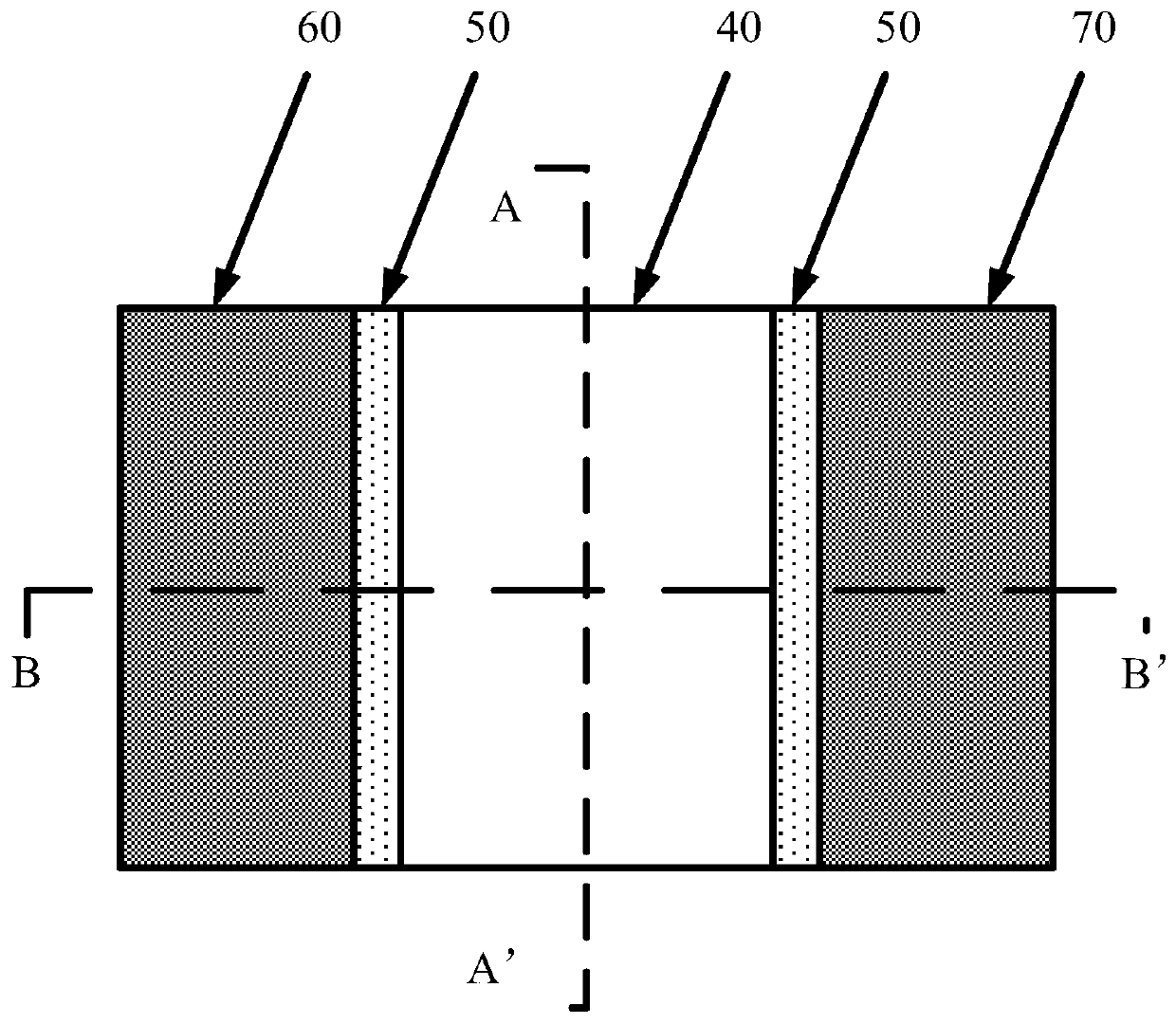
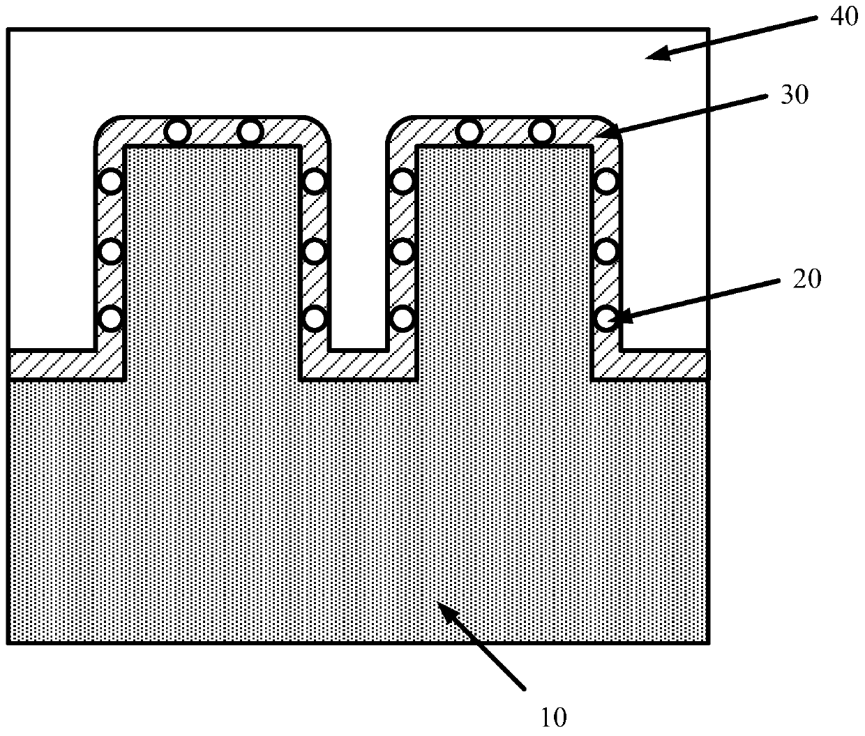
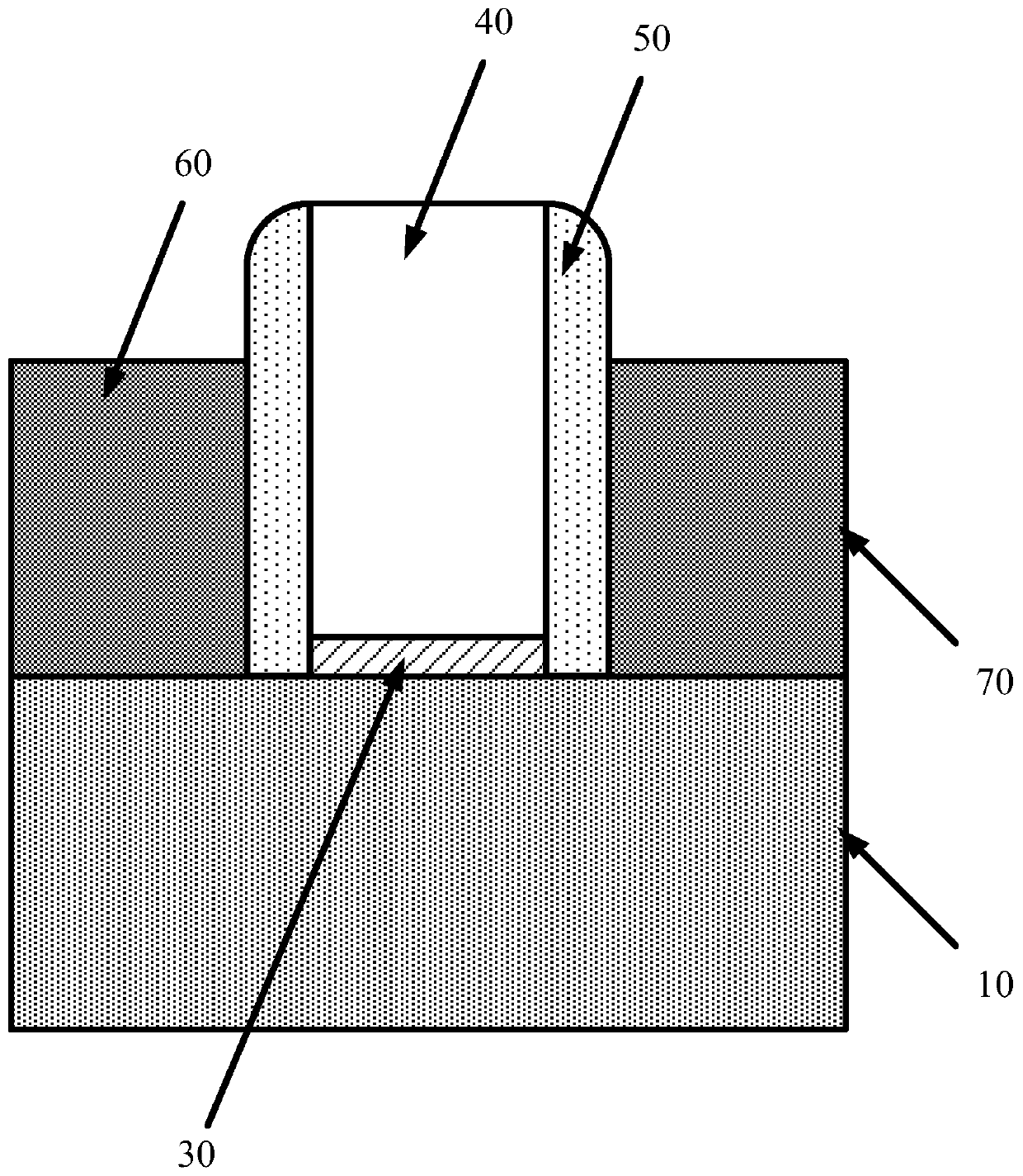
[0031] In order to further improve the gate efficiency and drive current of the field effect transistor channel, refer to Figure 1-3 , a carbon nanotube three-dimensional fin transistor with a three-dimensional structure and using carbon nanotubes (Carbon Nanotubes) as a channel came into being, Figure 1-Figure 3 shows the general structure of this carbon nanotube 3D fin tr...


PUM


Abstract

The invention discloses a carbon nanotube three-dimensional fin transistor and a preparation method thereof. The carbon nanotube three-dimensional fin transistor is a transistor structure based on anembedded gate fin with Dirac two-dimensional semimetal as source and drain electrodes. The short channel effect of the carbon nanotube three-dimensional fin transistor can be reduced while the fin transistor has a small size, since the Dirac two-dimensional semimetal has a two-dimensional ultra-thin structure, the electrostatic shielding effect of the source and drain electrodes for a gate electrode in the gate structure can be reduced when the Dirac two-dimensional semimetal is used as source and drain electrode materials of the carbon nanotube three-dimensional fin transistor, and therefore,the short channel effect of the carbon nanotube three-dimensional fin transistor can be reduced. In addition, according to the carbon nanotube three-dimensional fin transistor, the potential distribution in a channel can be affected by applying a voltage to an embedded metal gate fin, therefore, the discrete regulation of a device threshold can be achieved, and the function of dynamically controlling the threshold of the device is achieved.

Description

technical field [0001] The present application relates to the field of semiconductor technology, and more specifically, relates to a carbon nanotube three-dimensional fin transistor and a preparation method thereof. Background technique [0002] Moore's Law means that when the price remains constant, the number of components that can be accommodated on an integrated circuit will double every 18-24 months, and the performance will also double. [0003] With the continuous shrinking of the size of semiconductor devices, it becomes more and more difficult for field effect transistors in traditional two-dimensional structure CMOS (Complementary Metal Oxide Semiconductor, Complementary Metal Oxide Semiconductor) integrated circuits to continue Moore's Law. And with the advancement of Moore's Law and the shrinking of the size of logic devices, the short-channel effect is becoming more and more obvious, such as the increase of the sub-threshold swing and the decrease of the potenti...

Claims


Application Information

Patent Timeline
IPC IPC(8): H01L29/78H01L29/45H01L29/16H01L21/336
CPCH01L29/16H01L29/45H01L29/66795H01L29/785
Inventor 徐琳张志勇彭练矛
Owner PEKING UNIV
Why Eureka
Try Eureka