Coupling structure of SiON waveguide and optical fiber and manufacturing method of structure
A technology of optical fiber coupling and manufacturing method, which is applied in the coupling of optical waveguide, optical guide, optics, etc., can solve the problem of large coupling loss between SiON waveguide and optical fiber, and achieve the purpose of expanding the size of optical mode field, reducing dispersion loss, and improving confinement ability Effect
- Summary
- Abstract
- Description
- Claims
- Application Information
AI Technical Summary
Problems solved by technology
Method used
Image

Examples
Embodiment 1
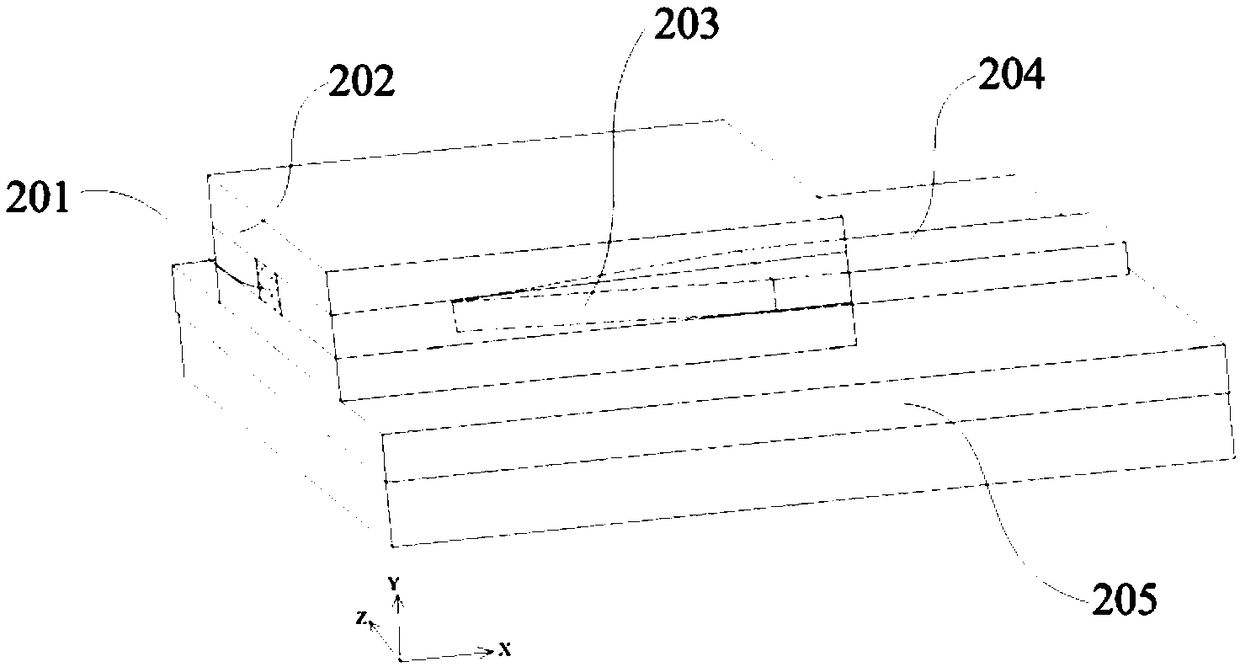
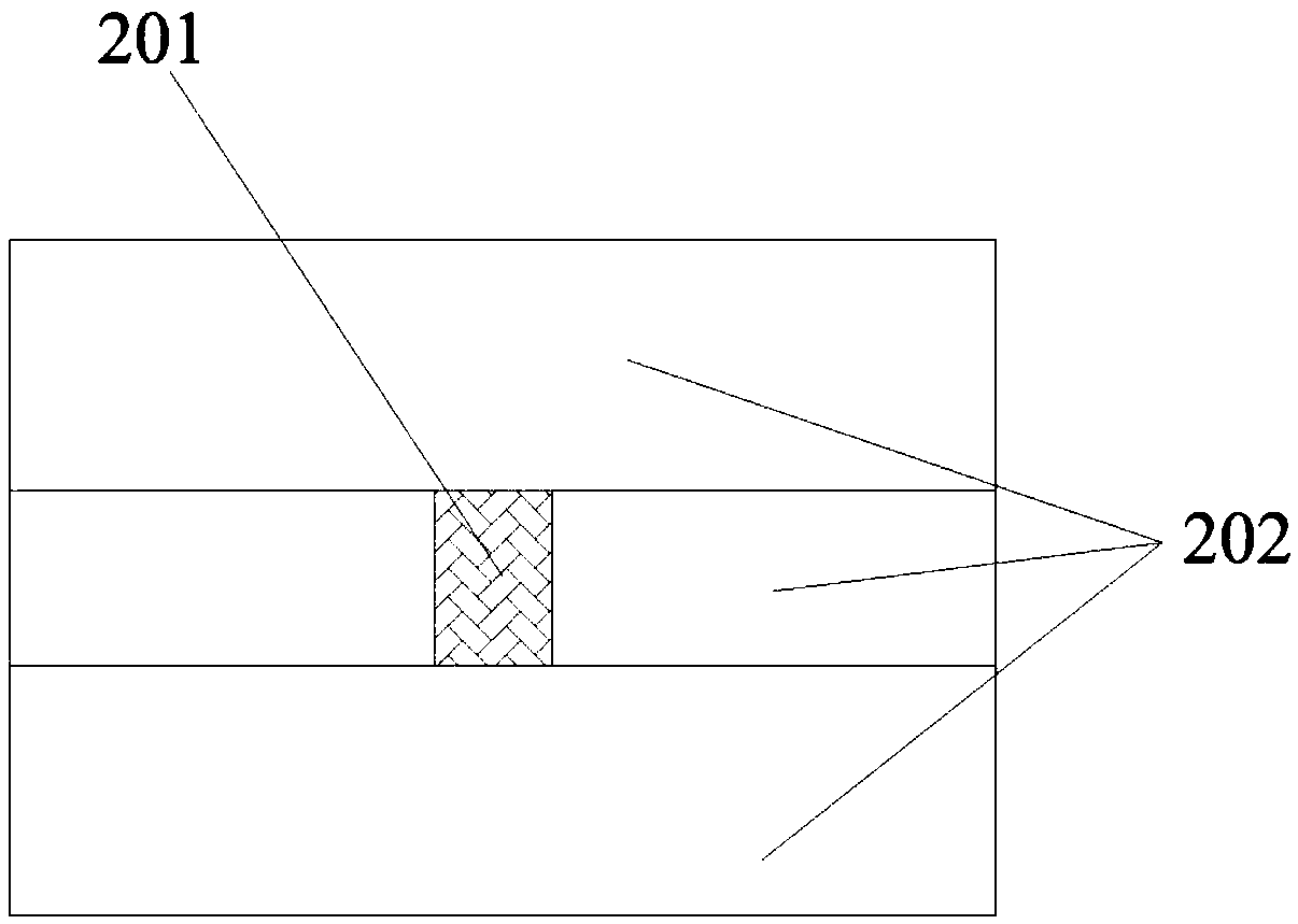
[0044] SiON waveguide and fiber coupling structure of the present invention, such as figure 2 with image 3 As shown, it includes SiON waveguide 201, which is an input waveguide; silicon dioxide waveguide 202, which is coated on the outside of SiON waveguide 201; tapered SiON waveguide 203201, which is coated on the inside of silicon dioxide waveguide 202, and is at the level of SiON waveguide 201 and the cross-sectional dimension is smaller than that of the SiON waveguide 201, and the cross-sectional dimension gradually expands along the direction of light transmission; the SiON output waveguide 204 is connected to the tapered SiON waveguide 203201.
[0045] Wherein, the SiON waveguide 201 is located where the symmetry axis of the silica waveguide 202 is located. The tapered SiON waveguide 203201 is located where the axis of symmetry of the silica waveguide 202 is located. The silicon dioxide waveguide 202 has a rectangular cross-section and is composed of a buried oxide l...
Embodiment 2
[0053] For the manufacture of the reverse tapered pattern converter, we used an SOI wafer with a top layer silicon thickness of 340nm and a BOX layer thickness of 2μm. The whole process of making is as follows:
[0054] S1: After the RCA process, clean the SOI wafer;
[0055] S2: Spin-coat the PMMA photoresist on the SOI wafer at a speed of 4000 rpm and a thickness of 220nm;
[0056] S3: Use Raith150 electron beam exposure machine, and after developing and fixing, make tapered structure, waveguide structure and mask patterns of alignment marks used in ordinary lithography overlay;
[0057] S4: Using ICP etching technology, transfer the mask pattern to the SOI wafer, and etch for 50s under shallow2LR3 etching conditions;
[0058] S5: Use the plasma glue machine to remove the residual glue, and clean the SOI wafer with RCA;
[0059] S6: cover a layer of SiON capping layer with PECVD, the refractive index is 1.7, and the thickness is 3 μm;
[0060] S7: Spin-coat photoresist o...
PUM
 Abstract
Description
Claims
Application Information
 - Generate Ideas
- Intellectual Property
- Life Sciences
- Materials
- Tech Scout
- Unparalleled Data Quality
- Higher Quality Content
- 60% Fewer Hallucinations
Browse by: Latest US Patents, China's latest patents, Technical Efficacy Thesaurus, Application Domain, Technology Topic, Popular Technical Reports.
© 2025 PatSnap. All rights reserved.Legal|Privacy policy|Modern Slavery Act Transparency Statement|Sitemap|About US| Contact US: help@patsnap.com