Method for improving efficiency of coupling waveguide and fiber

A technology of optical fiber coupling and waveguide, which is applied in the field of improving the coupling efficiency of waveguide and optical fiber, can solve the problems of light field leakage, substrate leakage loss, leakage, etc., achieve small optical field mismatch loss, eliminate leakage loss, and improve coupling efficiency Effect

Inactive Publication Date: 2010-12-29
INST OF SEMICONDUCTORS - CHINESE ACAD OF SCI
View PDF3 Cites 1 Cited by
  • Summary
  • Abstract
  • Description
  • Claims
  • Application Information

AI Technical Summary

Problems solved by technology

Usually, after the waveguide (including the inverted tapered end) is fabricated, a layer of silicon dioxide is deposited to protect the waveguide. This structure is equivalent to the coupling between a nanowire waveguide buried in a flat medium and an optical fiber, and there will be a large The light field leaks into the flat plate region
At the same time, since the thickness of the buried silicon dioxide of the SOI sheet is about 1 to 3um, and the exit mode field radius of the tapered optical fiber is also about 2um, part of the optical signal will leak to the substrate silicon when the optical fiber is coupled to the waveguide. , resulting in substrate leakage loss

Method used


Image

  • Method for improving efficiency of coupling waveguide and fiber
  • Method for improving efficiency of coupling waveguide and fiber
  • Method for improving efficiency of coupling waveguide and fiber

Examples


Embodiment Construction

[0023] In order to make the object, technical solution and advantages of the present invention clearer, the present invention will be described in further detail below in conjunction with specific embodiments and with reference to the accompanying drawings.

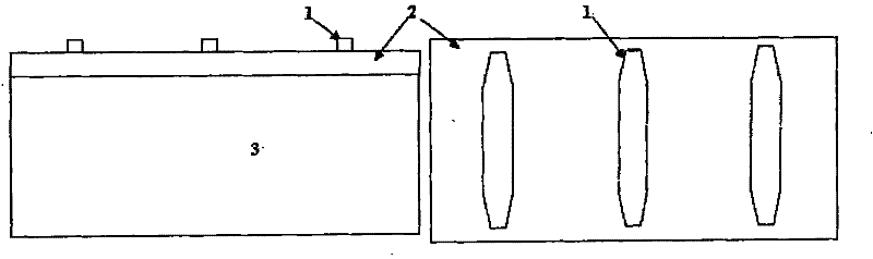
[0024] Figure 1 (a) is the overall schematic diagram of the nanowire waveguide device after it is made. The nanowire waveguide is made on the SOI wafer, 1 is the silicon nanowire waveguide, made on the top silicon of the SOI wafer, and 2 is the buried layer 2 of the SOI wafer. Silicon oxide, the thickness of the silicon dioxide layer is 1 to 3 microns, 3 is the substrate silicon of the SOI wafer.

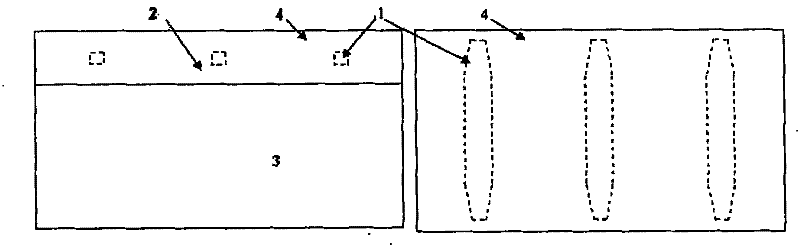
[0025] Figure 1(b) is the overall schematic diagram of silicon dioxide deposited on the surface of the device, which is deposited on the surface of the fabricated nanowire waveguide 1 by using the plasma-enhanced chemical vapor deposition PECVD process, using silane and nitrous oxide at 350 Celsius reaction to generate silicon ...


PUM


Abstract

The invention relates to a method for improving efficiency of coupling waveguide and fiber. The method comprises the following step: depositing silicon dioxide on the surface of the manufactured waveguide to fully wrap the waveguide; then, etching the silicon dioxide to a silicon underlayer to form a coupling end structure of wrapping silicon waveguide by silicon dioxide waveguide; and then, etching the silicon underlayer inwards by 10 to 50 microns to form a suspended coupling end structure of wrapping the silicon waveguide by the silicon dioxide waveguide with the thickness of between 10 and50 microns. The method effectively improves the limiting capacity of the coupling structure to an optical field, reduces the dispersion loss of an end head with an inverse tapered coupling structure,removes the leakage loss of the optical field to the underlayer after the diffusion of the optical field and improves the coupling efficiency with the fiber.

Description

technical field [0001] The invention relates to a method for improving the coupling efficiency of the silicon-based nanowire waveguide and the optical fiber by etching the silicon dioxide waveguide and etching the coupling end substrate silicon. Background technique [0002] Traditional silicon-based large-section waveguides cannot integrate multiple optical functional devices on a single SOI chip due to their large bending radius (on the order of hundreds of microns to millimeters), which limits the development of large-scale integrated optical circuits. Therefore, silicon-based nanowire waveguides arouse people's attention and research. As the cross-section of silicon-based waveguides becomes smaller and smaller, the coupling of optical signals between waveguides and optical fibers becomes more and more difficult. The cross-sectional area of ​​silicon-based nanowire waveguides is 0.1um 2 order of magnitude, while the core diameter of single-mode fiber is 254.5um 2 , rega...

Claims


Application Information

Patent Timeline
Patent Type & Authority Patents(China)
IPC IPC(8): G02B6/136G02B6/12
Inventor 耿敏明张磊贾连希杨林刘育梁
Owner INST OF SEMICONDUCTORS - CHINESE ACAD OF SCI
Why Eureka
Try Eureka