A method for extracting parasitic parameters of a silicon carbide inverter

A technology of parasitic parameters and inverters, applied in the direction of instruments, electrical digital data processing, special data processing applications, etc., can solve the problems of prolonging the production cycle, increasing production costs, and increasing the probability of rework, so as to reduce the probability of rework and reduce production Cost, effect of improving accuracy

Active Publication Date: 2019-03-08
HUAZHONG UNIV OF SCI & TECH
View PDF2 Cites 1 Cited by
  • Summary
  • Abstract
  • Description
  • Claims
  • Application Information

AI Technical Summary

Problems solved by technology

[0003] At present, the parasitic parameters of the inverter are often measured by instruments such as impedance analyzers after the finished inverter is processed, but no corresponding measures are taken to accurately extract the parasitic parameters of the inverter during the design process. This will not only increase the production cost, but also Increase the chance of rework, thereby extending the production cycle

Method used


Image

  • A method for extracting parasitic parameters of a silicon carbide inverter
  • A method for extracting parasitic parameters of a silicon carbide inverter
  • A method for extracting parasitic parameters of a silicon carbide inverter

Examples


Embodiment Construction

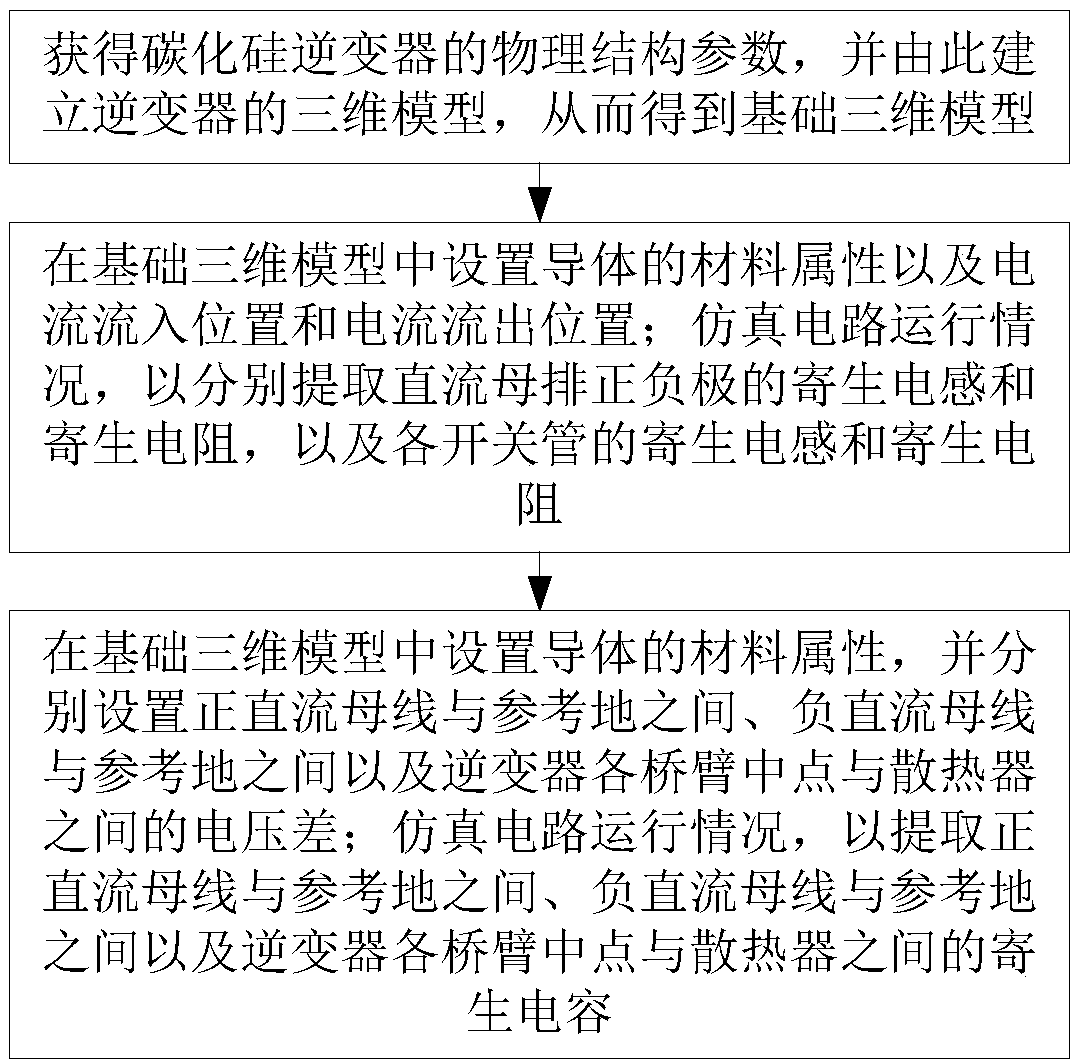
[0028] In order to make the object, technical solution and advantages of the present invention clearer, the present invention will be further described in detail below in conjunction with the accompanying drawings and embodiments. It should be understood that the specific embodiments described here are only used to explain the present invention, not to limit the present invention. In addition, the technical features involved in the various embodiments of the present invention described below can be combined with each other as long as they do not constitute a conflict with each other.

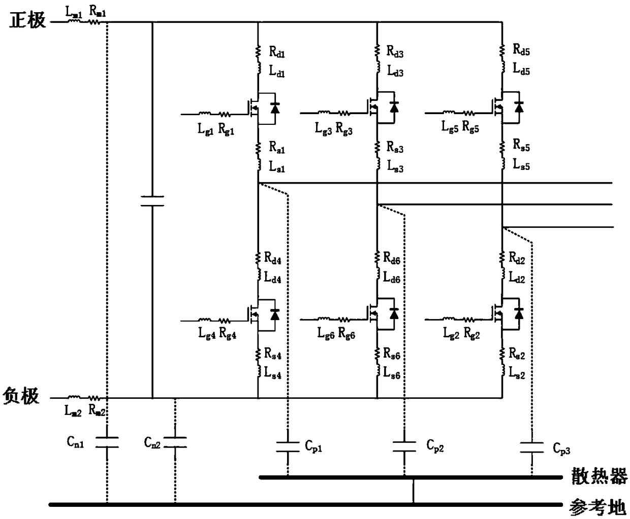
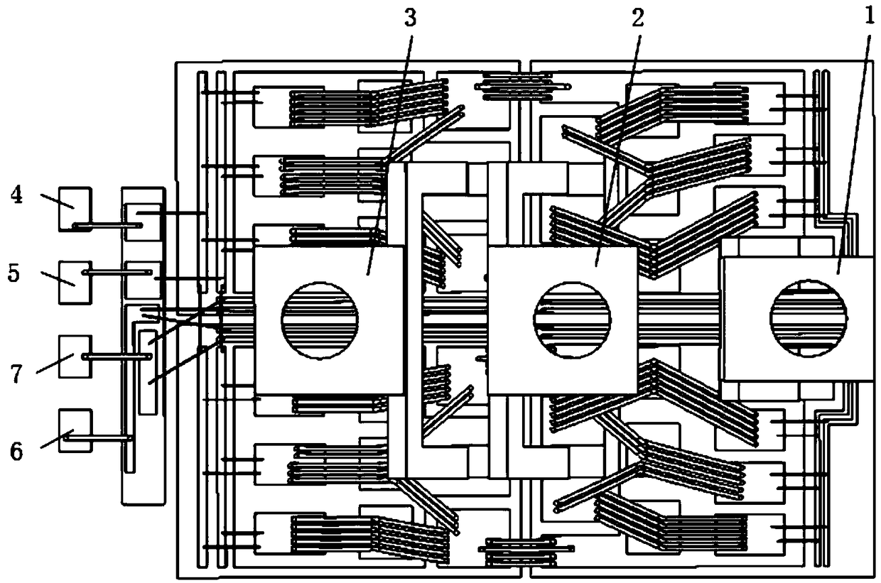
[0029] In the present invention, the physical structure of the silicon carbide inverter and the parasitic parameters that need to be extracted are as figure 1 As shown, the switching tubes on the three-phase bridge arms are all silicon carbide (SiC) MOSFETs (Metal-Oxide-Semiconductor Field-Effect Transistor, Metal-Oxide Semiconductor Field-Effect Transistor), and the parasitic parameters that ne...


PUM


Abstract

The invention discloses a method for extracting parasitic parameters of a silicon carbide inverter, which comprises the following steps of obtaining physical structure parameters of the silicon carbide inverter, and thereby establishing a three-dimensional model of the inverter, thereby obtaining a basic three-dimensional model; setting the material properties of conductor, current inflow positionand current outflow position in the basic three-dimensional model; simulating circuit operation to extract parasitic inductance and parasitic resistance; setting the material properties of the conductor in the basic three-dimensional model, and setting the voltage difference between the positive DC bus and the reference ground, the negative DC bus and the reference ground, and the voltage difference between the middle point of each bridge arm of the inverter and the heat sink respectively; and simulating circuit operation to extract parasitic capacitance. The methd of the invention can accurately extract the parasitic parameters of the inverter through a software simulation method in the design process of the inverter, so as to reduce the production cost and shorten the manufacturing period.

Description

technical field [0001] The invention belongs to the field of inverters, and more specifically relates to a method for extracting parasitic parameters of a silicon carbide inverter. Background technique [0002] Wide bandgap semiconductor silicon carbide (SiC) power devices have the advantages of high power density, low switching loss, suitable for high-frequency operation, and good high-temperature stability. In the past ten years, SiC power electronic devices have developed rapidly. Mainstream semiconductor manufacturers have Invest in related research and development and production. However, due to the fast switching speed of silicon carbide devices, the resulting spike voltage may affect the driving signal, and even endanger equipment and personal safety. Therefore, it is necessary to extract the parasitic parameters inside the inverter, and then determine the measures to reduce the parasitic parameters to improve electromagnetic compatibility. [0003] At present, the ...

Claims


Application Information

Patent Timeline
Patent Type & Authority Applications(China)
IPC IPC(8): G06F17/50
CPCG06F30/398G06F30/367Y02B70/10
Inventor 孔武斌高学鹏曲荣海于子翔俞志跃高慧达
Owner HUAZHONG UNIV OF SCI & TECH
Why Eureka
Try Eureka