Metal oxide film and preparation method thereof, thin film transistor and array substrate

A technology of oxide thin film and anodization, which is applied in transistors, electric solid state devices, semiconductor devices, etc., and can solve the problem of uneven brightness of display panels

Inactive Publication Date: 2019-03-12
HEFEI XINSHENG OPTOELECTRONICS TECH CO LTD +1
View PDF4 Cites 2 Cited by
  • Summary
  • Abstract
  • Description
  • Claims
  • Application Information

AI Technical Summary

Problems solved by technology

[0003] The main purpose of the present invention is to provide a metal oxide thin film and its preparation method, a thin film transistor and an array substrate to solve the problem of uneven brightness at different positions of the display panel in the related art

Method used


Image

  • Metal oxide film and preparation method thereof, thin film transistor and array substrate
  • Metal oxide film and preparation method thereof, thin film transistor and array substrate

Examples


Embodiment Construction

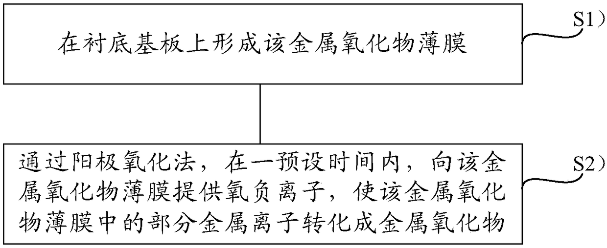
[0020] The following will clearly and completely describe the technical solutions in the embodiments of the present invention with reference to the accompanying drawings in the embodiments of the present invention. Obviously, the described embodiments are only some, not all, embodiments of the present invention. Based on the embodiments of the present invention, all other embodiments obtained by persons of ordinary skill in the art without making creative efforts belong to the protection scope of the present invention.

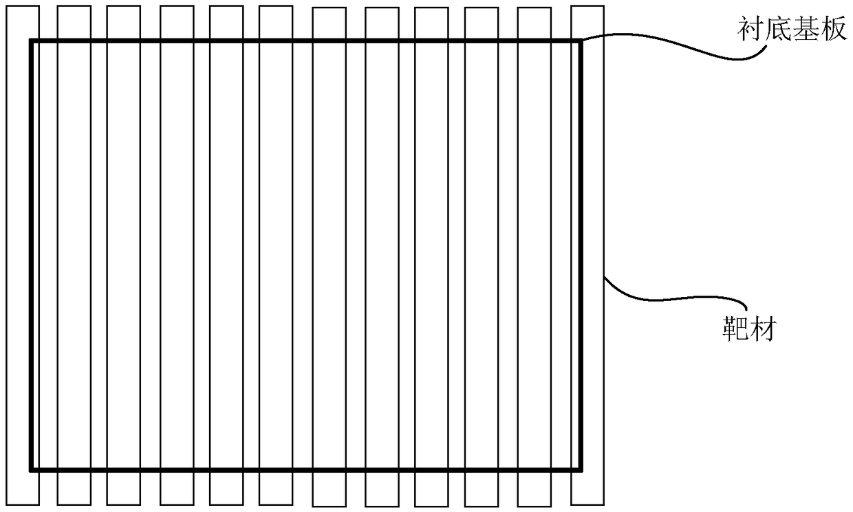
[0021] Generally, there are two main methods for preparing the metal oxide thin film of the semiconductor active layer. The first is the vacuum method, which is to use the magnetron sputtering equipment to accelerate the metal oxide target to the cathode under the action of an electric field through argon ions, and The surface of the metal oxide target is bombarded with high energy, so that the target particles are sputtered and deposited on the substrate to fo...


PUM


Abstract

The invention relates to the field of a display technique, and in particular to a metal oxide film and a preparation method thereof, a thin film transistor and an array substrate. The metal oxide filmand the preparation method thereof, the thin film transistor and the array substrate are used for solving the problem of uneven brightness of different positions of the display panel in the related art. The embodiment of the present invention provides the preparation method of the metal oxide film. The preparation method comprises the steps of forming the metal oxide film on an underlayer substrate; and providing an oxygen anion to the metal oxide film by using an anodic oxidation method within preset time so that part of metal ions in the metal oxide film are converted into metal oxides. Theembodiment of the invention is used for manufacturing of the display panel.

Description

technical field [0001] The invention relates to the field of display technology, in particular to a metal oxide thin film and a preparation method thereof, a thin film transistor and an array substrate. Background technique [0002] At present, a thin film transistor (Thin Film Transistor, TFT) is a main driving element of an active matrix liquid crystal display and an active matrix organic light emitting diode (AMOLED). Among them, the quality of the semiconductor active layer directly affects the performance of the thin film transistor. Contents of the invention [0003] The main purpose of the present invention is to provide a metal oxide thin film and its preparation method, a thin film transistor and an array substrate, so as to solve the problem of uneven brightness at different positions of the display panel in the related art. [0004] To achieve the above object, the present invention adopts the following technical solutions: [0005] In the first aspect, an emb...

Claims


Application Information

Patent Timeline
Patent Type & Authority Applications(China)
IPC IPC(8): H01L21/363H01L29/24H01L29/786H01L27/12
CPCH01L21/02565H01L21/02631H01L21/02664H01L27/1225H01L29/24H01L29/7869H01L21/02422H01L21/02554H01L21/02628H01L29/66969
Inventor 宋威赵策金憘槻刘宁丁远奎李伟胡迎宾
Owner HEFEI XINSHENG OPTOELECTRONICS TECH CO LTD
Why Eureka
Try Eureka