Method for Electroplating Copper Layer on Lead Frame

A technology of lead frame and electroplated copper layer, which is applied in the field of lead frame electroplated copper layer, can solve the problem of weak bonding between electroplated copper layer and sealing glue, and achieve the effect of increasing the bonding strength and strengthening the degree of firmness

Active Publication Date: 2021-03-26
ACKOTEC ZHONGSHAN ELECTRONICS PARTS
View PDF5 Cites 0 Cited by
  • Summary
  • Abstract
  • Description
  • Claims
  • Application Information

AI Technical Summary

Problems solved by technology

[0003] Based on this, the present invention provides a method for electroplating a copper layer on a lead frame, which can effectively improve the problem of weak bonding between the electroplated copper layer and the sealant, and improve the bonding strength between the electroplated copper layer and the sealant

Method used


Image

  • Method for Electroplating Copper Layer on Lead Frame
  • Method for Electroplating Copper Layer on Lead Frame
  • Method for Electroplating Copper Layer on Lead Frame

Examples


Embodiment 1

[0062] This embodiment provides a method for electroplating a copper layer on a lead frame, comprising the following steps:

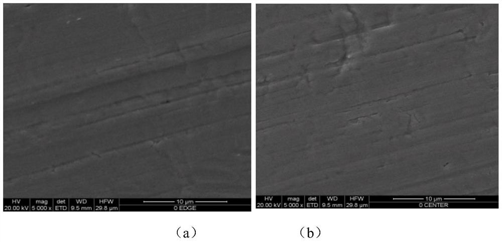
[0063] (1) Degreasing: figure 1 is the scanning electron microscope image of the substrate surface of the lead frame, where figure 1 (a) is a schematic diagram of the surface condition of the center part of the lead frame base material, figure 2 (b) is a schematic diagram of the surface condition at the edge of the lead frame substrate. Will figure 1The lead frame base material shown was electrolyzed in a PT-200 solution (PT-200 degreasing powder, purchased from Vico Matheson Co., Ltd.) with a concentration of 100g / L, with a current density of 3A / dm and a temperature of 50°C. The electrolysis time is 30s. After degreasing, wash the residue with tap water.

[0064] (2) Activation: at room temperature, soak the base material in the salt solution AS310 for 15s, the concentration of the salt solution is 80g / L, purchased from Zhongshan Anshun metal tre...

Embodiment 2

[0074] This embodiment provides a method for electroplating a copper layer on a lead frame, which is basically the same as Embodiment 1, except that the bidirectional pulse conditions are as shown in Table 2:

[0075] Table 2

[0076]

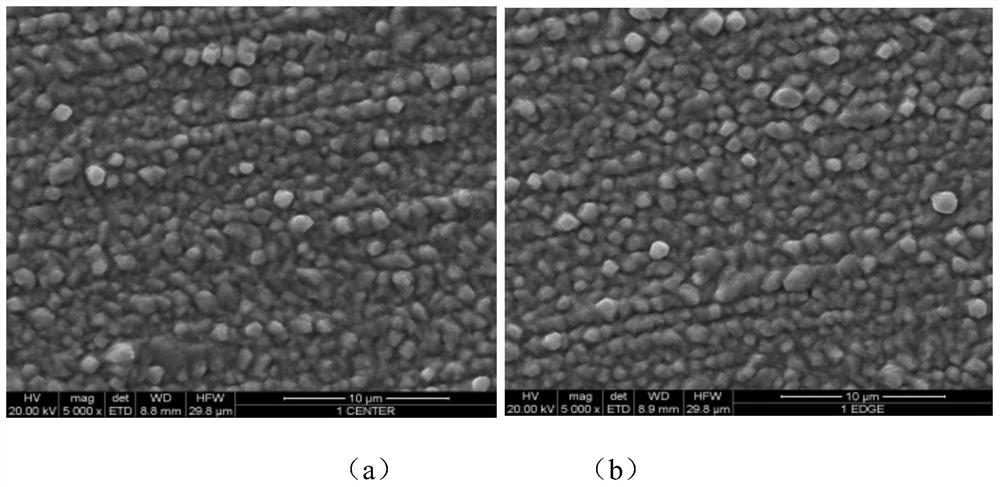
[0077] The scanning electron microscope figure of present embodiment copper layer surface is as image 3 as shown, image 3 (a) is a schematic diagram of the surface condition of the copper layer at the center of the lead frame, image 3 (b) is a schematic diagram of the surface condition of the copper layer at the edge of the lead frame. From image 3 It can be seen that the particle size on the surface of the copper layer in the center is small, the particle size distribution is uniform, and the roughness is small. The space between the surface particles of the copper layer at the edge position is large, the particle size distribution is uneven, and the roughness is large. As a result, when the glue is sealed, the bonding strength betw...

Embodiment 3

[0079] This embodiment provides a method for electroplating a copper layer on a lead frame, which is basically the same as Embodiment 1, except that the bidirectional pulse conditions are as shown in Table 3:

[0080] table 3

[0081]

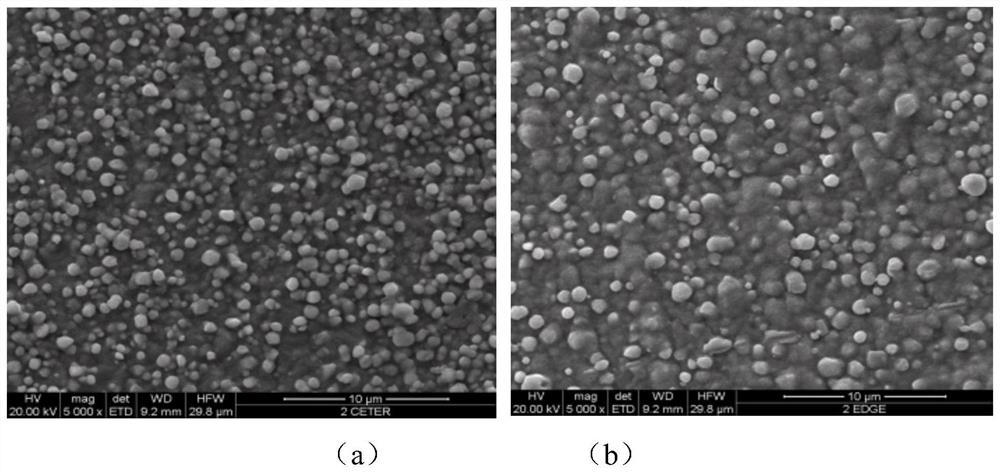
[0082] The scanning electron microscope figure of present embodiment copper layer surface is as Figure 4 shown. Figure 4 (a) is a schematic diagram of the surface condition of the copper layer at the center of the lead frame, Figure 4 (b) is a schematic diagram of the surface condition of the copper layer at the edge of the lead frame. From Figure 4 It can be seen that the particle size of the surface of the copper layer is small and the roughness is small. As a result, when the sealant is sealed, the bonding strength between the metal copper layer and the sealant is weak. After measurement, the thickness of the copper layer in this embodiment is 378.8nm-437.1nm.


PUM

PropertyMeasurementUnit
thicknessaaaaaaaaaa
thicknessaaaaaaaaaa
thicknessaaaaaaaaaa

Abstract

The invention relates to a method for electroplating a copper layer on a lead frame. The method comprises the following steps: pre-treating a lead frame substrate; electroplating the pretreated lead frame substrate by adopting bi-directional pulse current, to obtain a copper layer; and performing post-treatment on the copper layer to obtain the copper layer. The process parameters of the bi-directional pulse current include: the forward pulse with the current density being 10ASD-15ASD, and the pulse width being 0.5ms-50ms; the reverse pulse with the current density being minus 40ASD-minus 30ASD, and the pulse width being 0.1ms-10ms. The method can effectively improve the adhesive strength of the electro-coppering layer and a sealant.

Description

technical field [0001] The invention relates to the field of electroplating of integrated circuits, in particular to a method for electroplating a copper layer of a lead frame. Background technique [0002] As the chip carrier of the integrated circuit, the lead frame is a kind of electrical connection between the lead-out end of the internal circuit of the chip and the outer lead by means of bonding materials (gold wire, aluminum wire, copper wire), and is a key structural part to form an electrical circuit. It plays the role of a bridge connecting with external wires. Most of the semiconductor integrated blocks need to use lead frames, which is an important basic material in the electronic information industry. After the metal layer is plated on the surface of the lead frame, it is generally bonded with epoxy molding compound (EMC). At present, when the surface of the electroplated copper layer of the lead frame is sealed with glue, because the surface of the electroplate...

Claims


Application Information

Patent Timeline
Patent Type & Authority Patents(China)
IPC IPC(8): C25D5/18C25D3/38C25D7/00
CPCC25D3/38C25D5/18C25D7/00
Inventor 刘国强徐卉军
Owner ACKOTEC ZHONGSHAN ELECTRONICS PARTS
Why Eureka
Try Eureka