Trench insulated gate bipolar transistor device and generating method thereof

A bipolar transistor, insulated gate technology, applied in semiconductor devices, semiconductor/solid-state device manufacturing, electrical components, etc., can solve problems such as low gate-source voltage and thin gate oxide thickness at the bottom of trenches

Inactive Publication Date: 2019-03-15
上海擎茂微电子科技有限公司
View PDF7 Cites 4 Cited by
  • Summary
  • Abstract
  • Description
  • Claims
  • Application Information

AI Technical Summary

Problems solved by technology

In the existing trench technology, due to the unavoidable sharp shape of the bottom of the trench, the thickness of the ...

Method used


Image

  • Trench insulated gate bipolar transistor device and generating method thereof
  • Trench insulated gate bipolar transistor device and generating method thereof
  • Trench insulated gate bipolar transistor device and generating method thereof

Examples


Embodiment Construction

[0078] The application will be described in further detail below in conjunction with the accompanying drawings.

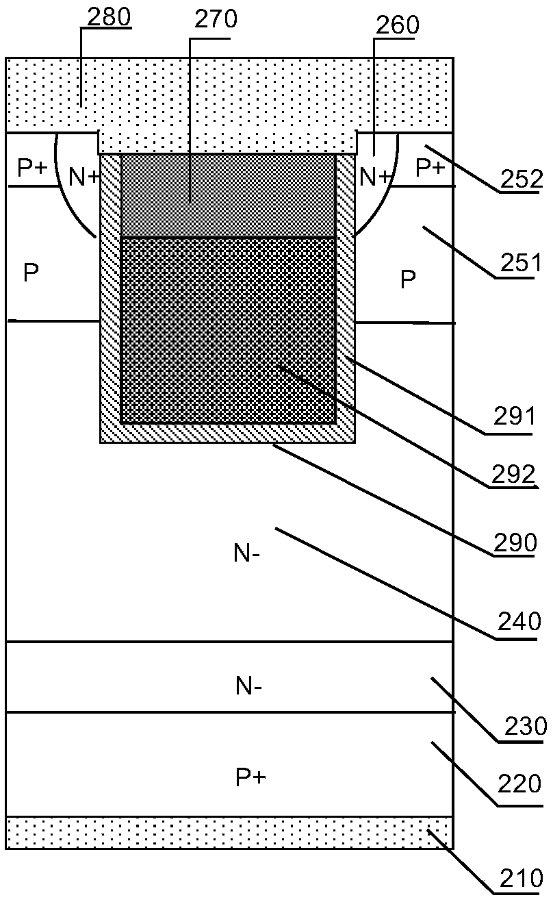
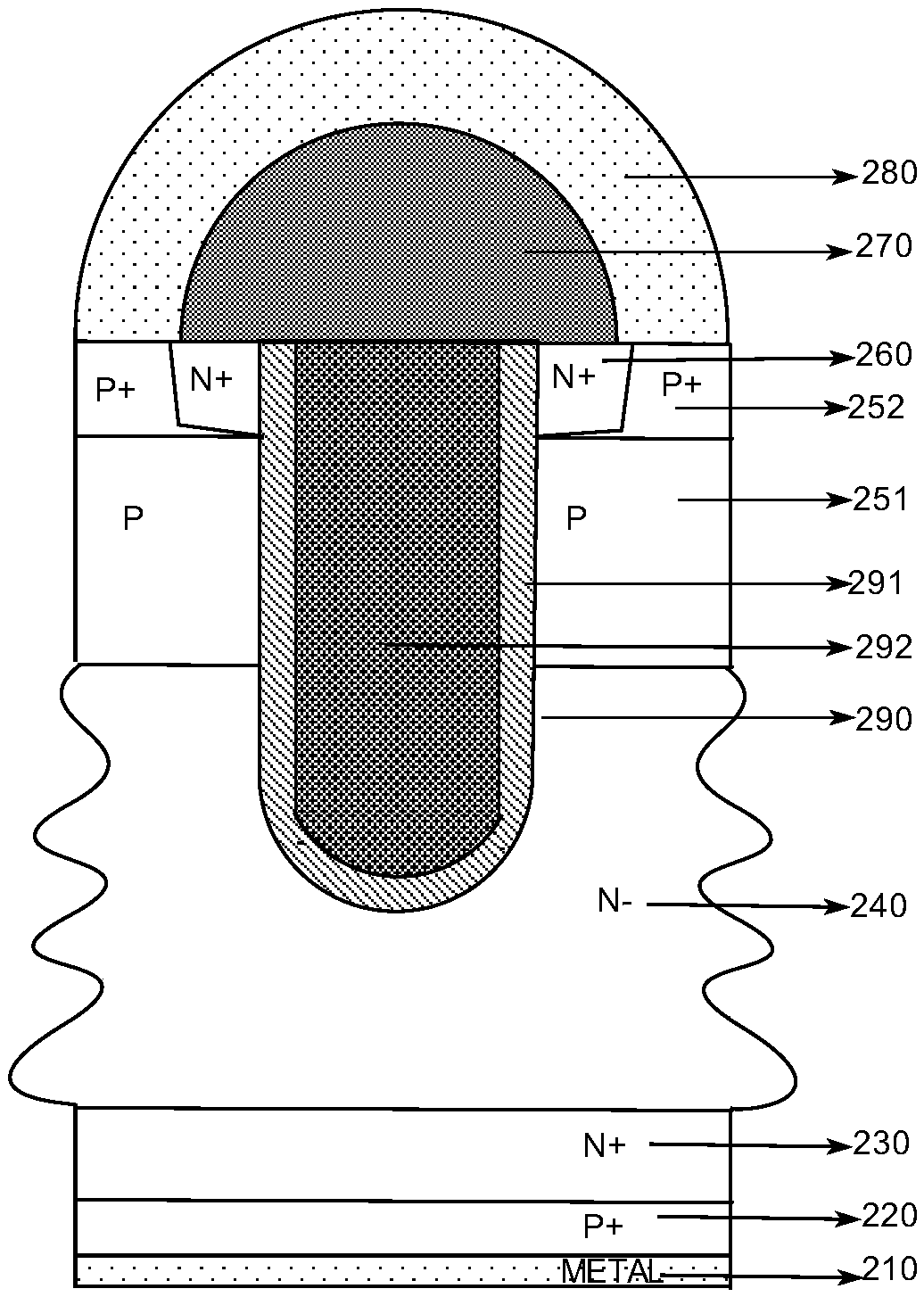
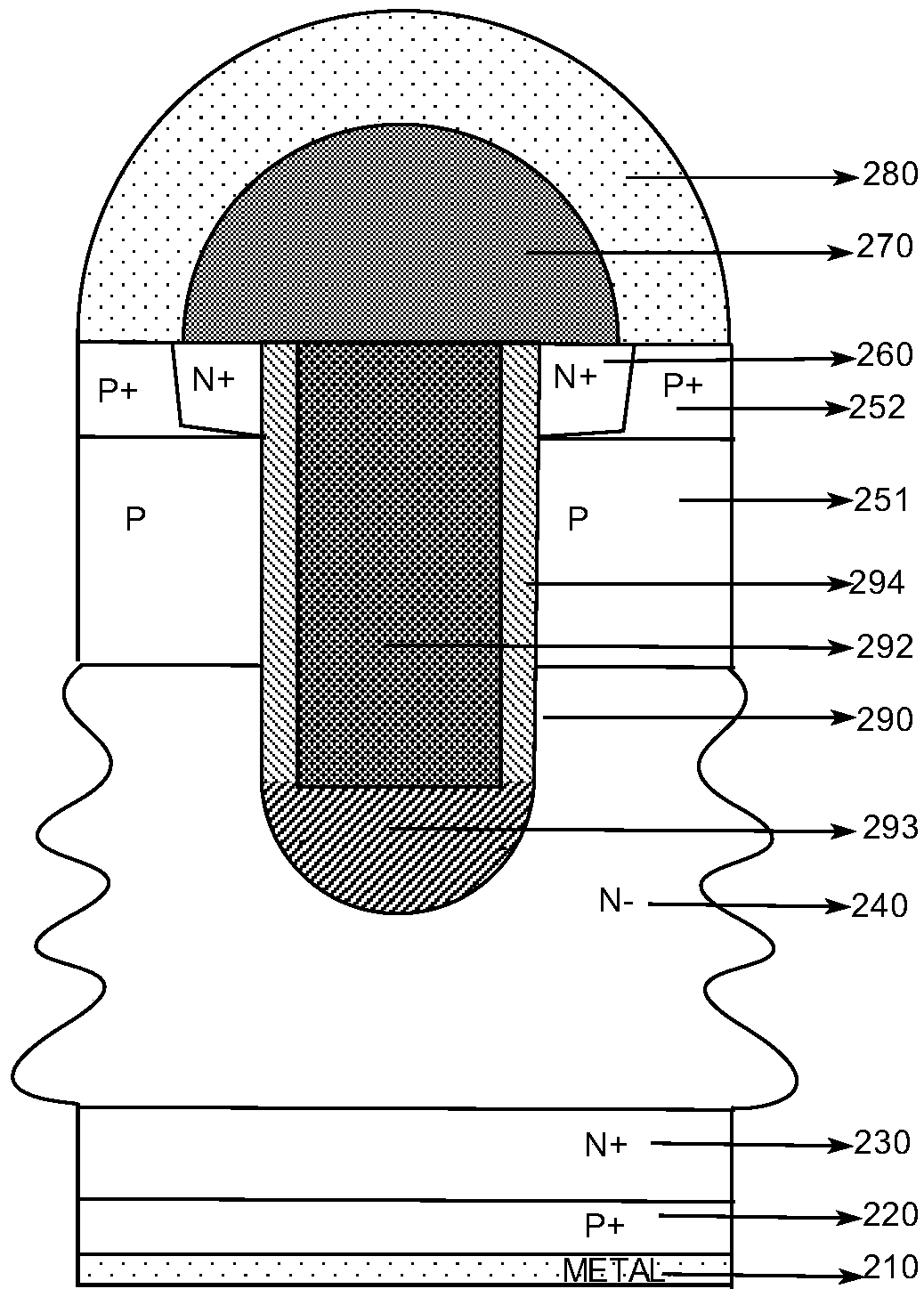
[0079] Such as image 3 As shown, the present application provides a trench insulated gate bipolar transistor device, comprising: a trench region 290, a gate oxide film 293 located at the bottom of the trench region 290, and a sidewall of the trench region 290 Gate oxide film 294, polysilicon gate 292, front emitter metal layer 280, silicon dioxide insulating dielectric layer 270, N+ emitter 260, P-type base region 251, P+ contact region 252, N-type base region 240, N-type The field termination region 230 and the P-type collector 220, the back collector metal layer 210, wherein,

[0080] The P-type base region 251 is formed on the surface of the N-type base region 240;

[0081] The polysilicon gate 292 is grown in the trench region 290, and the polysilicon gate 292 is a trench structure, which runs through the P-type base region 251 and the N-type base region 240...


PUM

PropertyMeasurementUnit
Thicknessaaaaaaaaaa
Thicknessaaaaaaaaaa

Abstract

The invention provides a trench insulated gate bipolar transistor device and a generating method thereof. A relatively thick gate oxide film is formed at the bottom of a trench region through a plasmafilm forming process. Due to the fact that the thickness of the gate oxide film at the bottom of a trench is increased, the consistency of the gate oxide thickness is guaranteed, the defect that a gate oxide layer at the bottom of the trench is easy to break down is eliminated, and the robustness of a gate oxide breakdown voltage is improved. Meanwhile, the area of a gate-drain capacitor is reduced, so that the Miller capacitance is reduced, the switch delay time is shortened, the switch dynamic loss of a device is reduced, and the switch characteristic of the device is improved. Meanwhile, the relatively thick gate oxide film is formed at the bottom of the trench, so that the upper surface of polycrystalline silicon subjected to back etching can be leveled and is slightly higher than thesurface of a silicon wafer of a N-type base region; and higher N+ emitter junction depth can be formed without increasing the injection energy of an N+ emitter and carrying out longer-time high-temperature trap pushing, so that the vertical overlapping area of the gate and the source is reduced, the gate-source capacitance is reduced, and the switch loss of an IGBT is reduced.

Description

technical field [0001] The present application relates to trench insulated gate bipolar transistor devices and methods of producing the same. Background technique [0002] Insulated Gate Bipolar Transistor (Insulated Gate Bipolar Transistor, hereinafter referred to as IGBT) is a Darlington structure semiconductor power power that combines a Metal Oxide Semiconductor Field Effect Transistor (MOSFET) and a Bipolar Junction Transistor (BJT). Electronic devices have the characteristics of voltage control, large input impedance, low driving power, small on-resistance, low switching loss and high operating frequency. They are ideal semiconductor power switching devices. The switching frequency is between 10-100KHZ and has broad application development and application prospects. [0003] Chinese patent CN103094324A discloses a novel IGBT device structure such as figure 1 As shown, the trench type IGBT consists of a trench region 290, a gate oxide layer 291, a polysilicon gate 292...

Claims


Application Information

Patent Timeline
IPC IPC(8): H01L29/739H01L29/423H01L21/331H01L21/28
CPCH01L29/401H01L29/4236H01L29/66348H01L29/7397H01L29/7398
Inventor 阳平
Owner 上海擎茂微电子科技有限公司
Why Eureka
Try Eureka