Passivation of laser facets and systems for performing the same

A facet and passivation layer technology, which is applied in the field of passivation of laser facets, can solve the problems of shortening laser life and increasing costs, and achieve the effects of less optical loss, prolonging life, and reducing reliability and life

Active Publication Date: 2019-03-15
TRUMP PHOTONICS
View PDF4 Cites 2 Cited by
  • Summary
  • Abstract
  • Description
  • Claims
  • Application Information

AI Technical Summary

Problems solved by technology

Extended operation of the laser at high output power generates heat, which in turn leads to degradation of one or more mirrors arranged at one or more facets of the laser
Resulting mirror damage reduces laser lifetime and increases cost due to the need to acquire replacement lasers

Method used


Image

  • Passivation of laser facets and systems for performing the same
  • Passivation of laser facets and systems for performing the same
  • Passivation of laser facets and systems for performing the same

Examples


Embodiment Construction

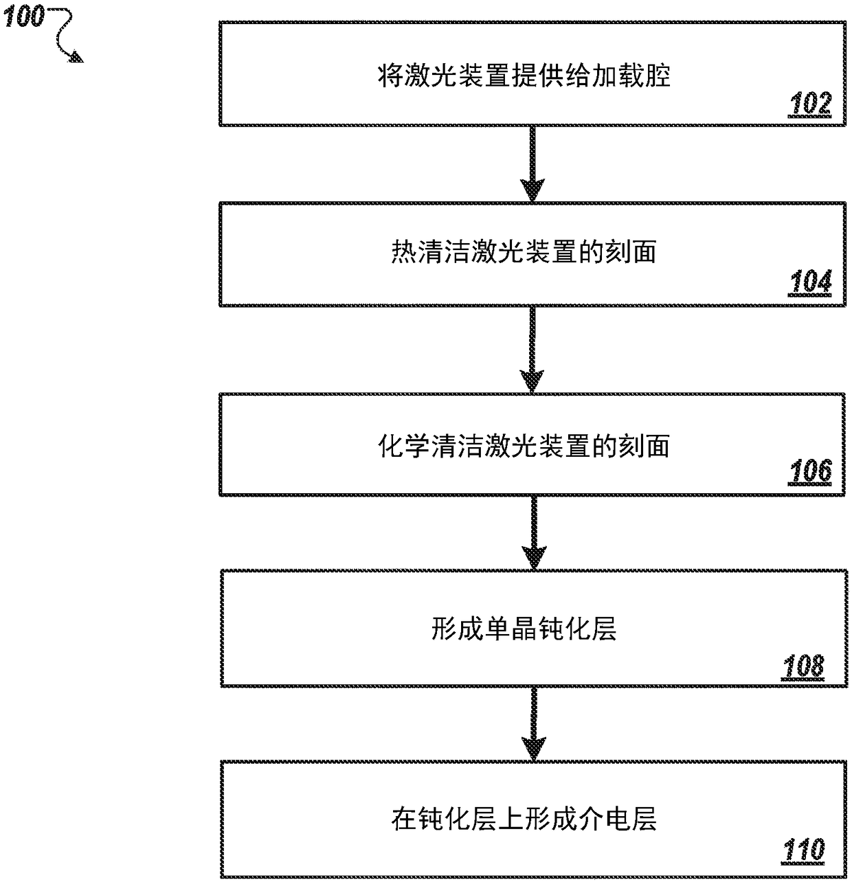
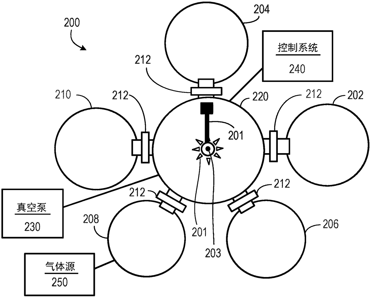
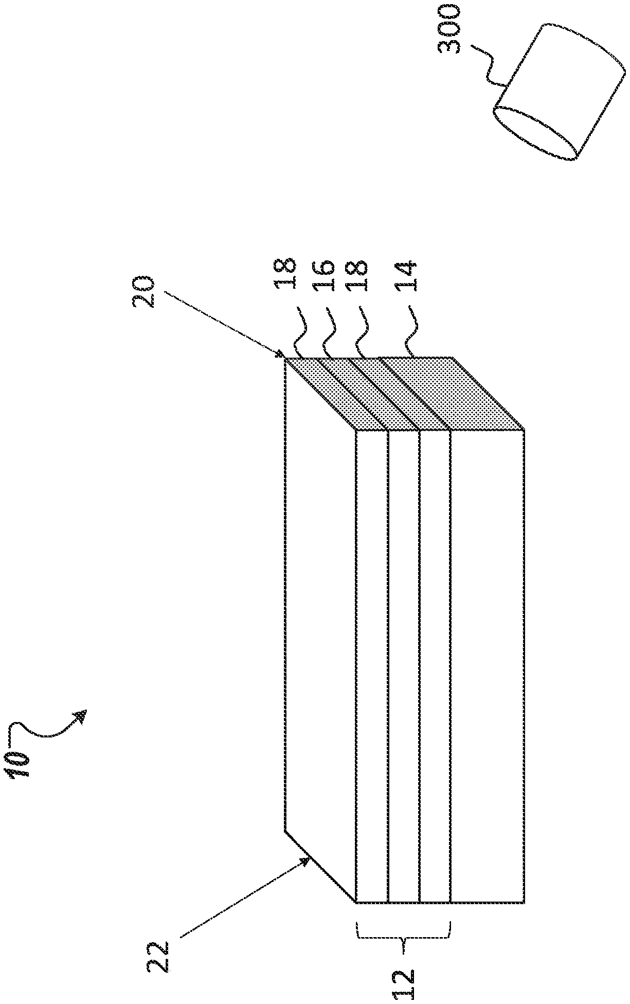
[0035] figure 1 An example of a process 100 for fabricating a high quality semiconductor laser facet passivation layer is shown. figure 2 An integrated multi-chamber ultra-high vacuum (UHV) system 200 is shown in which process 100 may be performed. Figure 3-6 Different states of the laser device 10 that have been enhanced to passivate the process 100 are shown.

[0036] like figure 2 As shown, the integrated multi-chamber UHV system 200 includes a central chamber 220 and a plurality of secondary chambers ( 202 , 204 , 206 , 208 , 210 ), each coupled to the central chamber through a corresponding gate valve 212 . The gate valve includes a passage through which objects can move and which can be sealed to maintain a vacuum. Gate valve 212 may be configured for use in a UHV environment and to isolate the secondary chamber from central chamber 220 . The plurality of secondary chambers includes, for example, a degassing chamber 202, a device inversion chamber 204, an atomic h...


PUM

PropertyMeasurementUnit
thicknessaaaaaaaaaa
widthaaaaaaaaaa

Abstract

Methods of passivating at least one facet of a multilayer waveguide structure can include: cleaning, in a first chamber of a multi-chamber ultra-high vacuum (UHV) system, a first facet of the multilayer waveguide structure; transferring the cleaned multilayer waveguide structure from the first chamber to a second chamber of the multi- chamber UHV system; forming, in the second chamber, a first single crystalline passivation layer on the first facet; transferring the multilayer waveguide structure from the second chamber to a third chamber of the multi-chamber UHV system; and forming, in the third chamber, a first dielectric coating on the first single crystalline passivation layer, in which the methods are performed in an UHV environment of the multi-chamber UHV system without removing themultilayer waveguide structure from the UHV environment.

Description

technical field [0001] The present invention relates to passivation of laser facets and a system for performing passivation of laser facets. Background technique [0002] Semiconductor lasers are electro-optical devices that convert electrical energy into light and are used in a variety of applications such as optical communication systems, laser printers, disk drives, and the like. High power semiconductor lasers are especially useful in laser processing applications. A major root cause of failure of high power diode lasers is known as catastrophic optical mirror damage (COMD), which typically occurs after the diode laser has been operated at high power output for extended periods of time. Prolonged operation of the laser at high output power generates heat, which in turn leads to degradation of one or more mirrors arranged at one or more facets of the laser. The resulting mirror damage shortens laser lifetime and increases cost due to the need to acquire replacement lase...

Claims


Application Information

Patent Timeline
Patent Type & Authority Applications(China)
IPC IPC(8): H01S5/028
CPCC23C14/021C23C14/568H01J37/32743H01J37/32899C30B23/02H01S5/4025H01S5/0282H01S5/0281H01S5/34313H01S5/0287H01J37/32082C30B29/48H01S5/10H01J37/32889H01J37/32816C30B23/066C23C14/46H01J2237/327H01J2237/335
Inventor Q·张H·安H·G·特罗伊施
Owner TRUMP PHOTONICS
Why Eureka
Try Eureka