MEMS resonant pressure sensor based on Si-Si-Si-glass wafer bonding technology and manufacturing process thereof

A si-si-si-, pressure sensor technology, applied in the field of resonant pressure sensor sensitive chips, can solve problems such as long-term stability, reliability, manufacturing process difficulty, etc., to ensure high quality factors, reduce residual stress and heat. Effects of stress, improved accuracy and stability

Active Publication Date: 2019-03-19
BEIJING RES INST OF TELEMETRY +1
View PDF9 Cites 11 Cited by
  • Summary
  • Abstract
  • Description
  • Claims
  • Application Information

AI Technical Summary

Problems solved by technology

[0009] The purpose of the present invention is to overcome the shortcomings of the existing MEMS silicon resonant pressure sensor in terms of long-term stability, reliability, and manufacturing process difficulty, and provide a high-precision and high-precision sensor based on Si-Si-Si-glass four-layer wafer bonding technology. Stable MEMS resonant pressure sensor reduces the manufacturing process difficulty of high-vacuum wafer packaging and long-term vacuum maintenance, and the accuracy, stability and reliability of the sensor are significantly improved

Method used


Image

  • MEMS resonant pressure sensor based on Si-Si-Si-glass wafer bonding technology and manufacturing process thereof
  • MEMS resonant pressure sensor based on Si-Si-Si-glass wafer bonding technology and manufacturing process thereof
  • MEMS resonant pressure sensor based on Si-Si-Si-glass wafer bonding technology and manufacturing process thereof

Examples


Embodiment

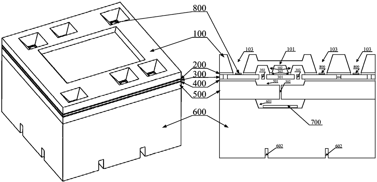
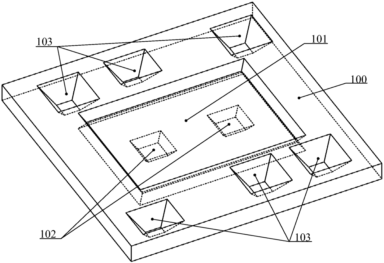
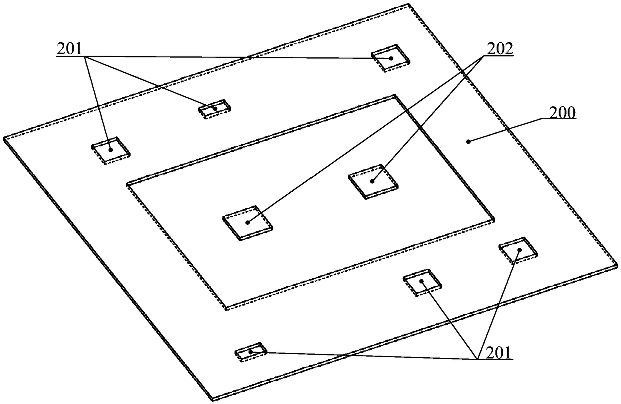
[0073]The Si pressure-sensitive layer 100 is made of ultra-low resistivity (2 The layer is fabricated based on an oxide layer below the Si pressure sensitive layer 100 with a thickness of 0.8 μm. The thickness of the Si resonator layer is 60 μm, the resistivity is ±0.2Ω·cm within a certain value in the range of 0.1Ω·cm to 5Ω·cm, (100) crystal orientation, and P-type silicon. Second SiO 2 The layer is fabricated based on an oxide layer above the Si pit substrate layer 500 with a thickness of 0.8 μm. The Si pit substrate layer is made of ultra-low resistivity (-6 ~3.5×10 -6 . The depth of the pit structure 601 is 50 μm, the depth of the topological stress isolation strip groove structure 602 is 0.8 mm, the topological form is a well-shaped grid, and the getter film 700 is a Ti metal film with a thickness of 500 nm.

[0074] Such as Figure 8 ~ Figure 18 It is the MEMS manufacturing process step of the sensor of the present invention.

[0075] (1) Figure 8 Shown is a schem...


PUM

PropertyMeasurementUnit
thicknessaaaaaaaaaa
electrical resistivityaaaaaaaaaa
thicknessaaaaaaaaaa

Abstract

The invention discloses a MEMS resonant pressure sensor based on Si-Si-Si-glass wafer bonding technology and a manufacturing process thereof. The order of the MEMS resonant pressure sensor from top tobottom is a Si pressure sensitive layer, a Si resonator layer, a Si pit substrate layer, a glass pit substrate layer, a Si pressure sensitive layer and a Si resonator layer. The Si resonator layer and the Si pit substrate layer are bonded by a Si-Si bonding process. The Si pit substrate layer and the glass pit substrate layer are bonded by a Si-glass anodic bonding process. A first SiO2 layer isarranged between the Si pressure sensitive layer and the Si resonator layer, and a second SiO2 layer is arranged between the Si resonator layer and the Si pit substrate layer. According to the MEMS resonant pressure sensor of the invention, the process difficulty of MEMS micro-nano processing and high vacuum packaging is reduced; residual stress and thermal stress are effectively reduced; reliability and vacuum and long-term maintenance of the vacuum reference cavity are improved; temperature compensation accuracy is improved; the overall accuracy and stability of the pressure sensor is improved.

Description

technical field [0001] The invention belongs to the field of sensitive chips of resonant pressure sensors, in particular to a high-precision and high-stability MEMS resonant pressure sensor based on Si-Si-Si-glass four-layer wafer bonding technology. Background technique [0002] High-precision, high-stability pressure sensors are used in new generation fighters, large transport aircraft and civil aviation airliners, space stations and deep space and extraterrestrial planet detection, submarines and deep-sea submersibles, aerospace and missile weapons, vacuum pipeline high-speed vehicles, meteorological observation, Consumer electronics and other fields have a wide range of application requirements. The resonant pressure sensor is the one with the highest comprehensive accuracy, the best temperature stability and long-term stability among all kinds of pressure sensors, and has been widely recognized by the academic research field and the industry. Micro-Electro-Mechanical S...

Claims


Application Information

Patent Timeline
Patent Type & Authority Applications(China)
IPC IPC(8): B81C1/00B81B7/02G01L1/14G01L1/18
CPCB81B7/02B81B2201/0264B81B2203/0118B81C1/0038B81C1/00666B81C1/0088B81C2201/0191G01L1/148G01L1/18
Inventor 焦海龙郭伟龙杨挺郝文昌金小锋尹玉刚
Owner BEIJING RES INST OF TELEMETRY
Why Eureka
Try Eureka